|
MEMS technology
- Non-reflecting surfaces
- Patterned polymer samples were made by casting a poly(dimethylsiloxane) stamp from the silicon nanospike surface and then UV or hot embossing an ...
today Materials Views - MEMS technology
- Sandia's RapTOR System Seeks to Quantify "Unknown Unknown" Biothreats - 17th ...
- The Knowledge Foundation has announced that Sandia National Laboratories' Dr. Steven S. Branda will present a paper entitled "Microfluidics-Based Systems ...
yesterday San Francisco Chronicle (press release) - MEMS technology
- Solar film holds big promise
- "(The thin film process) is the same thing, only on a much larger scale with many drops that are arranged in an array," Shreve said. ...
today New Mexican - MEMS technology
- Easy Fabrication of Non-Reflecting and Self-Cleaning Silicon and Plastic Surfaces
- 4, 2010) — The Microfabrication group of Aalto University which specializes in microfabrication and microfludics has developed a new and rapid method for ...
yesterday Science Daily (press release) - MEMS technology
MEMS business
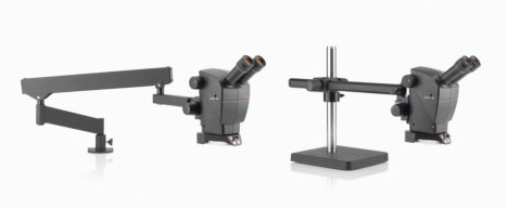
 Leica A60 S and A60 F - New Stereomicroscopes Increase Productivity in ... Leica A60 S and A60 F - New Stereomicroscopes Increase Productivity in ...
- (Nanowerk News) Leica Microsystems is bringing its new A series to the market especially for the requirements in production of printed circuit boards or ...
today Nanowerk LLC - MEMS business
- MEMtronics receives Missile Defense Agency contract for microwave phase ...
- "These circuits take advantage of MEMtronics' developments in radio frequency microelectromechanical systems (RF MEMS) technology, which have been ...
today Nanotechnology News (press release) - MEMS business
- Tegal Receives Repeat Order for Tegal 3200 SE Silicon DRIE Process Module from ...
- The Company's plasma etch tools enable sophisticated manufacturing techniques, such as 3D interconnect structures formed by intricate silicon etch, ...
today Trading Markets (press release) - MEMS business
- Development of Ultra-Compact Microchip Packaging Technology by ...
- The FO-WLP production process is consist of formation of redistribution layer (RDL) with copper pillar bumps (CPB) on a support wafer, high-speed chip-to-wafer bonding using chips with electroless plated pads, and high-productive ...
sia yesterday - MEMS business
- New PinPoint® MEMS gyro - outstanding performance for low budgets
- By I-MicroNews A new class of small precision MEMS navigation and pointing gyros is now available to automotive, consumer and industrial customers wanting ...
yesterday R & D Magazine - MEMS business
 HP pursues 'sensing-as-a-service' HP pursues 'sensing-as-a-service'
- Hewlett Packard Co. is actively pursuing "sensing as a service" in future applications of its micro-electro-mechanical system (MEMS) expertise, according to ...
today EETimes.com - MEMS business
Nanotechnology
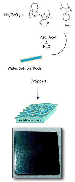
 Low-cost, hybrid thermoelectrics Low-cost, hybrid thermoelectrics
- Using simple water-based chemistry to wrap a polymer that conducts electricity around a nanorod of tellurium, this composite nanoscale thermoelectric is ...
today Nanowerk LLC - Nanotechnology
Featured Process
 MNX offers commercial e-beam lithography services using a state-of-the-art Vistec EBPG 5000+ direct-write tool. This affordable service provides you with the best performance and fastest turnaround times in the industry. | - 50MHz scan speed
- Spot size below 2.5 nm
- Large scan field size
- Fast cycle times
|
Event Calendar
|
|