|
MEMS technology
- 3D IC, WLP & TSV : Building Up In 3D: the steps from SOC to 3D-ICs
- By I-MicroNews Stacked die are expected to begin showing up in volume in late 2012 and in 2013, turning what has been a science experiment into a mainstream ...
today R & D Magazine - MEMS technology
- Discera's Silicon Oscillators Are The First To Deliver 10 ppm Accuracy For ...
- Their 2.6 billion hour MTBF reliability rating is over 2x better than the MEMS industry and is over 20x better than crystal oscillators with over 30x better ...
today Business Wire (press release) - MEMS technology
MEMS business
- Analog Devices Wins MEMS Microphone Patent Case
- "Since bringing our first MEMS microphone products to market in 2008, ADI has maintained our focus on innovation and providing the highest performance MEMS ...
today MarketWatch (press release) - MEMS business
- ESA Employs Goodrich Gyroscopes for Space Mission
- Goodrich Corporation's micro electro mechanical system (MEMS) gyros that were used in the satellite of the European Space Agency (ESA) named the Earth ...
today AZoSensors - MEMS business
 CCD Imaging Sensors with Ultra-High IR Sensitivity from Hamamatsu CCD Imaging Sensors with Ultra-High IR Sensitivity from Hamamatsu
- By employing the company's patented laser processing technology, a microelectromechanical systems design on the rear side of the CCD imager can be obtained, ...
today AZoSensors - MEMS business
- 3D, 4G and laser projectors: We look to the future of mobile phones
- Microvision already has a pocket(ish)-sized stand-alone laser projector, using a tiny micro-electromechanical (MEMS) mirror to combine the light from ...
today CNET UK - MEMS business
Nanotechnology
- CNT Annual Conference on Carbon Nanomaterials
- The focus will be on applications and technological requirements for carbon nanomaterials, especially in the fields of lightweight construction, mobility, ...
today Nanowerk LLC - Nanotechnology
- Lab Adds Nanoscale Layers on Silicon for Semiconductors | Science ...
- Researchers have integrated layers of the material indium arsenide onto a silicon substrate to create a nanoscale transistor with working electronic properties.
Alan today - Nanotechnology
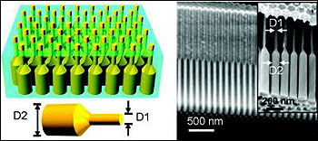
 Future Bright for Nanopillar Light Collectors Future Bright for Nanopillar Light Collectors
- Nanopillars — densely packed nanoscale arrays of optically active semiconductors — have shown potential for providing a next generation of relatively ...
today Photonics.com - Nanotechnology
- Nanomemory – Devices Based on Nanotubes and Nanowires
- Nanoscale memory devices are key elements of future nanoelectronics circuits. For improved performance, the down-scaling of both the size and the ...
today Materials Views - Nanotechnology
- Ultrathin alternative to silicon for future electronics | Science Blog
- “Moving forward we believe that the XOI substrates can be obtained through a wafer bonding process, but our technique should make it possible to fabricate both p- and n- type transistors on the same chip for complementary electronics ...
bjs today - Nanotechnology
Featured Event
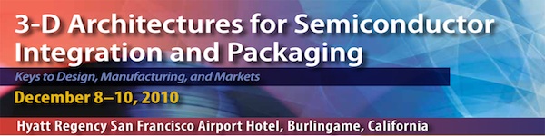 This conference gives a broad, yet thorough perspective on the technomarket opportunity and challenge offered by building devices and systems in the vertical dimension. Industry leaders from around the world are invited to speak at this conference on a wide range of topics important to the emerging and on-going 3-D integration and packaging.
Visit here for details and register today!
Event Calendar
|
|