|
View Mailing Online
MEMS technology
- Altering surface textures in 'counterintuitive manner' may lead to cooling ...
- VIDEO: These images show droplets being deposited on silicon surfaces that are smooth (top) and that have micro-scale silicon posts placed either close together (middle) or relatively far apart (bottom). At..
yesterday EurekAlert (press release) - MEMS technology
- Sensors from A to Z
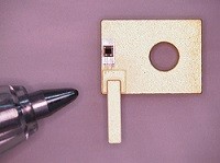
- The pair used the LIS331DLH Micro Electro-Mechanical Systems (MEMS) chip, and compared it with the earthquake sensor EpiSensor EST force balance accelerometer: they found the chip managed to pick-up earthquake vibrations greater than Magnitude ...
yesterday E&T magazine - MEMS technology
 Photon Fair 2013: Hamamatsu announces commercially viable photonic crystal ... Photon Fair 2013: Hamamatsu announces commercially viable photonic crystal ...
- ... applications, such as direct laser micro-fabrication, various types of laser excitation, wavelength conversion in projectors, sensing and measurement, position detection, distance-measuring image sensors, profile measurement systems and motion-sensing.
today Novus Light Technologies Today - MEMS technology
- Picodeon ColdAb Ultra-Short Pulsed Laser Deposition Systems Enable Thinner ...
- Precious metals like gold and platinum are finding more and more industrial applications in memory storage, energy harvesting, energy storage and microelectromechanical systems (MEMS) applications. Traditional production methods for thin gold films ...
today Azom.com - MEMS technology
 iPad Air: BOM of USD 304 iPad Air: BOM of USD 304
- Apple has exclusively utilized analog microphones in all its smartphones and tablets—except for the iPad 2, which sported a digital microelectromechanical system (MEMS) microphone from Analog Devices Inc. In another major departure, Apple is employing ...
today evertiq.com - MEMS technology
MEMS business
- Point-and-Shoot MEMS Analysis - An Interview with Jeremy Chen
- Across industries, we will start seeing more MEMS and NEMS sensors. As the design and fabrication process becomes faster, easier, and more standardized, I believe we will see more custom-designed sensors tailored specifically for their application.
today Azom.com - MEMS business
- Guest Blog: Design Enablement and the Emergence of the Near ...
- Guest blog post written by: Peter Himes, Silex Microsystems; Introduced by: Karen Lightman, MEMS Industry Group I am pleased to bring you this blog by Silex Microsystem's Peter Himes, vice president marketing & strategic ...
MEMS Industry Group yesterday - MEMS business
Nanotechnology
- 3D Printing Goes Nanoscale
- The process creates tiny, nanoscale-layered structures, tens of nanometers to hundreds of nanometers wide, formed one atom at a time. The nanscale allow structures made of a wide variety of materials and materials combinations, and with very high purity.
yesterday Design News - Nanotechnology
 Superfluidity Exists at Nanoscale Superfluidity Exists at Nanoscale
- Scientists at EPFL have provided the first experimental evidence of superfluidity at the nanoscale, shedding light on the fundamental basis of the phenomenon. Superfluidity refers to a state in which matter behaves like a liquid with zero viscosity ...
yesterday Laboratory Equipment - Nanotechnology
- Leveraging the nanoscale for greener lighting
- Mudring received a 'Proof-of-Concept' grant called BrightEMIL (EMIL goes green - exceptional materials from ionic liquids for energy saving applications in photonics') to test in particular the potential of ionic liquids as new solvents for generating ...
today Nanowerk - Nanotechnology
Nanotech business
 Graphite For EV Li-ion Batteries Could Be North America-Sourced Graphite For EV Li-ion Batteries Could Be North America-Sourced
- Northern Graphite explained the initial focus is on the development of nano-material based surface coatings for SPG. SPG is manufactured from flake graphite concentrate produced by graphite mines and is the anode material in li-ion batteries. Prices ...
yesterday Hybrid Cars News - Nanotech business
Featured Event
Participate at the premier conference for the lithography community. Contribute your latest work in the areas of advanced etch technology for nanopatterning, EUV lithography, microlithography, resist materials, and more. For the past 38 years, SPIE Advanced Lithography symposium has played a key role in bringing the lithography community together to solve challenges required by the semiconductor industry. Register today.
Event Calendar
|
|