|
View Mailing Online
MEMS technology
- Korean Team Develops Microfluidic Chip Integrating RNA Extraction, cDNA ...
- Researchers at Inje University in South Korea have developed a microfluidics-based chip that integrates three PCR needs into one device. The chip, which is about the size of a microscope slide, performs mRNA extraction, cDNA synthesis, and gene ...
today GenomeWeb - MEMS technology
- Zygo 3D optical profiler enhances surface metrology
- ... a wide range of application capabilities that include the metrology of roughness, flatness, angles, steps, and more, for applications ranging from precision-machined automotive components to patterned semiconductor wafers, to microfluidics and MEMS.
today Compound Semiconductor - MEMS technology
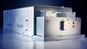
 Spectra-Physics Launch Quasar 355-60 UV Pulse Laser at Photonics West 2014 Spectra-Physics Launch Quasar 355-60 UV Pulse Laser at Photonics West 2014
- The new Quasar 355-60 transforms microelectronic device manufacturing, enabling major advances in both throughput and precision. “Quasar 355-60 is an astonishing leap forward in performance and capability that propel mobile device manufacturing and ...
yesterday Azom.com - MEMS technology
- iPhone 5 MEMS Microphones
- Apple initiated the trend of integrating three MEMS microphones with the iPhone 5. Two manufacturers compete to integrate their analog microphones, Knowles which largely dominates the MEMS microphone market (with half of the business) and AAC which ...
today PR Newswire (press release) - MEMS technology
 UV laser for micromachining UV laser for micromachining
- Ditzingen, Germany – Trumpf is showing the new TruMicro 3340 for the first time at SPIE Photonics West 2014. With this new design, the laser manufacturer is now offering a version of the nanosecond laser operating in the ultraviolet spectrum that can ...
today Industrial Laser Solutions Magazine - MEMS technology
- Femtosecond Laser Processing Enhances Medical Device Applications
- PLYMOUTH, Minn., Feb. 4, 2014 — LSA Laser now offers femtosecond laser processing capabilities for medical device manufacturing. This will prove particularly useful in micromachining applications for drilling and cutting high-precision holes and ...
yesterday Photonics.com - MEMS technology
 Satellite sensors to be used in medical systems, says Imec Satellite sensors to be used in medical systems, says Imec
- It uses a narrow-band spectral filters at pixel level using semiconductor thin-film processing, which cuts size and weight of the hardware and allows it to be mass produced in volume at low cost. Such sensor technology will allow camera vendors to ...
today ElectronicsWeekly.com - MEMS technology
- Breathalyser Applications of MEMS Sensors
- A microelectromechanical (MEMS) system is in general technology of very small devices, which range from 20µm to 1mm in size. This article explains the use of the MEMS sensor MiCS-5521 and the MiCS-5524 (Figures 1 and 2) in breathalyser applications.
yesterday AZoSensors - MEMS technology
MEMS business
- MEMS Cost Model and MEMS Price Model | Electronics.ca ...
- AKM (Asahi Kasei Microdevices) Noboka 3. APM (Asia Pacific Microsystems Inc.) Fab 1 4. APM (Asia Pacific Microsystems Inc.) Fab 2 5. Colibrys Ltd. None 6. Dalsa 100mm Line 7. Dalsa 150mm Line 8. Freescale Sendai Fab
Electronics.ca Publications today - MEMS business
- Opportunities and Implications for Indoor Energy Harvesting
- Production of microelectromechanical devices for EH ability and Internet of Things (IoT) with EH are expected to be key trends in the building technologies industry. • The forecast for building level controllers shipment for North America and Europe ...
today DigitalJournal.com - MEMS business
- Reverse Costing Analysis of the iPhone 5S MEMS Gyroscope ...
- STMicroelectronics 4x4mm MEMS gyro was integrated in the previous iPhones (iPhone 4, 4S & 5). For the new iPhone 5S, Apple has chosen the latest 3x3mm MEMS gyro from ST, thus achieving a 45% footprint reduction. The new 3-Axis MEMS gyroscope is ...
today SYS-CON Media (press release) - MEMS business
- Reverse Costing Analysis for the Bosch Sensortec BMG160 3-Axis MEMS ...
- Although the manufacturing process (Epi-poly surface micromachining) is similar to the one of automotive gyro, new processes for the capping and the wafer bonding has been adopted. Indeed, the classic "glass-frit" wafer bonding has been abandoned in ...
today SYS-CON Media (press release) - MEMS business
 Entegris agrees to buy ATMI in deal valued at $1.15 billion Entegris agrees to buy ATMI in deal valued at $1.15 billion
- In November, ATMI hired Barclays Capital to explore strategic options after demand for the company's materials waned in some markets such as microelectronic wafers. Entegris, a maker of liquid and gas filters and purifiers for the semiconductor ...
yesterday The Advocate - MEMS business
Nanotechnology
 Nanotechnology-enabled smartphone-based mercury testing Nanotechnology-enabled smartphone-based mercury testing
- (Nanowerk News) A team of researchers from the UCLA Henry Samueli School of Engineering and Applied Science has developed a smartphone attachment and application to test water for the presence of mercury, a toxic heavy metal. The new platform ...
today Nanowerk - Nanotechnology
 Nanotechnology is getting closer to 3D nanoprinting Nanotechnology is getting closer to 3D nanoprinting
- Applying 3D printing concepts to nanotechnology could bring similar advantages to nanofabrication – speed, less waste, economic viability – than it is expected to bring to manufacturing technologies. In addition, pre-patterned micro- or nanostructures ...
today Nanowerk - Nanotechnology
 Scientists produce first ever atom-by-atom simulation of ALD nanoscale film growth Scientists produce first ever atom-by-atom simulation of ALD nanoscale film growth
- Researchers at Tyndall National Institute, Ireland, have produced the first ever atom-by-atom simulation of nanoscale film growth by atomic layer deposition (ALD)—a thin-film technology used in the production of silicon chips. Present in all ...
today R & D Magazine - Nanotechnology
- Using nanotechnology to protect grain exports
- (Phys.org) —University of Adelaide researchers are using nanotechnology and the fossils of single-celled algae to develop a novel chemical-free and resistance-free way of protecting stored grain from insects. The researchers are taking advantage of ...
yesterday Phys.Org - Nanotechnology
- Photodetector nanotechnology enables photos in low-light conditions, with use ...
- Dark and blurry low-light photos could soon be a thing of the past, thanks to SUNY College of Nanoscale Science and Engineering (CNSE) scientists who have developed ultrathin "nanosheets" that could dramatically improve imaging technology used in ...
today BioOptics World - Nanotechnology
Featured Event
Event Calendar
- SPIE Photonics West 2014
- 2014-02-01 - 2014-02-06
San Francisco, CA
|
|
- Collaboration & Intellectual Property (IP) Management
- 2014-02-05
Online 11:30 AM - 12:30 PM ET
|
|
- SPIE Advanced Lithography 2014
- 2014-02-23 - 2014-02-27
San Jose, CA
|
|
- IEEE SF Bay Area MEMS Chapter
- 2014-02-26
Qualcomm Cafe @ Building B, 3165 Kifer Road, Santa Clara, CA 95051
7:45 PM to 8:45 PM. FBAR and FMOS Technology from a MEMS Perspective
|
|
- MEMS Executive Congress Europe 2014
- 2014-03-11
Munich, Germany
|
|
- The 9th Annual IEEE International Conference on Nano/Micro Engineered and Molecular Systems
- 2014-04-13 - 2014-04-16
Honolulu, Hawaii, USA
|
|
- 2014 Biosensors & Analytics Conference
- 2014-04-23 - 2014-04-24
Cleveland, OH
Sensing the Future of Healthcare
|
|
- MEMS Industry Group Conference
- 2014-04-24
Tokyo, Japan
The Global MEMS Supply Chain
|
|
- MIG M2M Forum 2014
- 2014-05-20 - 2014-05-21
Berkeley, CA
The MEMS Supply Chain - It Takes a Village
|
|
- Design Automation Conference (DAC 2014)
- 2014-06-01 - 2014-06-05
San Francisco, CA
|
|
- Hilton Head 2014
- 2014-06-08 - 2014-06-14
Hilton Head Island, SC
A Solid-State Sensors, Actuators and Microsystems Workshop
|
|
- Sensors Expo & Conference
- 2014-06-24 - 2014-06-26
Rosemont, IL
|
|
- MicroTAS 2014
- 2014-10-26 - 2014-10-30
San Antonio, TX
|
|
- The 28th International Conference on Micro Electro Mechanical Systems
- 2015-01-18 - 2015-01-22
Estoril, Portugal
|
|
- Transducers 2015
- 2015-06-21 - 2015-06-25
Anchorage, Alaska
|
|
|
|