|
View Mailing Online
MEMS technology
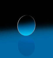
 Fused Silica Wafers measure quality of optical coatings. Fused Silica Wafers measure quality of optical coatings.
- July 11, 2014 - Exhibiting less than 10 Å surface roughness with surface quality of 40-20, TECHSPEC® Fused Silica Wafers are thin, circular pieces of UV fused silica designed to be used as test substrates to measure quality of optical coatings. Each is ...
2014-07-11 ThomasNet News (press release) - MEMS technology
- Getting a charge out of water droplets
- Chuanhua Duan, an assistant professor of mechanical engineering at Boston University who was not involved in this research, says, “This work provides a new approach for energy-harvesting, which can be used to power [microelectromechanical] devices ...
2014-07-13 MIT News - MEMS technology
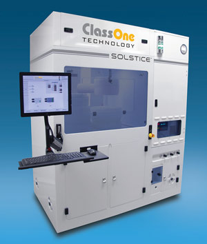
 ClassOne launches electroplating tool for smaller-substrate users ClassOne launches electroplating tool for smaller-substrate users
- ... of Kalispell, MT, USA has launched its Solstice line of electroplating tools, designed specifically for the smaller-substrate users in emerging technologies such as MEMS, LEDs, power devices, RF communications, interposers, photonics and microfluidics.
2014-07-11 Semiconductor Today - MEMS technology
- MEMS altitude pressure sensor detects 50-cm changes
- A highly-accurate absolute pressure sensor from Omron Electronic Components Europe can detect height differences of as little as 50cm. Based on Omron's MEMs technology, the tiny sensor module can measure altitude, atmospheric pressure or water depth ...
today EDN.com - MEMS technology
MEMS business
 For 'startup guy,' multiple bets on green energy For 'startup guy,' multiple bets on green energy
- When Fritzemeier later assisted with the launches of four or five enterprises using micro-electromechanical systems (MEMS) that were born in university laboratories, he became an expert in raising funds and building teams. “That's really where I got ...
yesterday California Lutheran University (blog) - MEMS business
- MEMS to be $8bn industry
- The proliferation of new multi-sensor platforms, Internet of Things applications and wearable technologies is expected to lift total MEMS semiconductor sales to a record $8billion in 2014. Despite a slump in 2012 and 2013, market research firm IC ...
today New Electronics - MEMS business
- THE 2014 SENSORS EXPO & CONFERENCE ACCLAIMED A ...
- ... AS THE LEADING SENSORS EVENT IN NORTH AMERICA: THE 2014
SENSORS EXPO & CONFERENCE ACCLAIMED A SUCCESS. July 1, 2014 ...
www.sensorsmag.com - MEMS business
 $1B USD Spent in Last Three Years on Silicon Photonics Acquisitions $1B USD Spent in Last Three Years on Silicon Photonics Acquisitions
- As the Si laser is probably years away from realisation, the different approaches are likely to be either attached laser (i.e., Luxtera) or indium-phosphide (InP) wafer-to-wafer/die-to-wafer bonding, followed by post-processing (i.e., Intel or Leti ...
today Novus Light Technologies Today - MEMS business
 Novartis signs deal with Google to bring smart lens tech to market Novartis signs deal with Google to bring smart lens tech to market
- According to Novartis, the partnership perfectly pairs the strengths of the two companies, as it marries Google's expertise in miniaturized electronics, low power chip design and microfabrication with Alcon's expertise in physiology, clinical ...
today ZDNet - MEMS business
Nanotechnology
 Diagnosing Type 1 Diabetes with Nanotechnology Diagnosing Type 1 Diabetes with Nanotechnology
- Described in a paper (“A plasmonic chip for biomarker discovery and diagnosis of type 1 diabetes”) published in Nature Medicine, the test employs nanotechnology to detect type 1 diabetes outside hospital settings. The handheld microchips distinguish ...
yesterday Genetic Engineering News - Nanotechnology
 With boron 'buckyball' find, nanotechnology advances With boron 'buckyball' find, nanotechnology advances
- With boron 'buckyball' find, nanotechnology advances. The discovery that a cluster of 40 boron atoms can form a hollow molecular 'cage' similar to a buckyball could be a nanotechnology game-changer. By: Bryan Nelson. Mon, Jul 14, 2014 at 02:50 PM.
yesterday Mother Nature Network - Nanotechnology
 Arrays of electrons trapped in nanoscale circuitry could form the basis for ... Arrays of electrons trapped in nanoscale circuitry could form the basis for ...
- Each of the dots in the device created by Delbecq's team was formed by three nanoscale metallic electrodes on a semiconductor substrate (Fig. 1). The capacitance between each dot couples the electron in one dot to that in the next, and the researchers ...
2014-07-11 Phys.Org - Nanotechnology
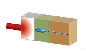
 New Insights on Fundamental Limits of Ultrafast Nanoscale Spintronic Devices New Insights on Fundamental Limits of Ultrafast Nanoscale Spintronic Devices
- A recent study by researchers at the University of Illinois at Urbana-Champaign provides new insights on the physical mechanisms governing the interplay of spin and heat at the nanoscale, and addresses the fundamental limits of ultrafast spintronic ...
2014-07-11 AZoNano.com - Nanotechnology
 3-D nanostructure could benefit nanoelectronics, gas storage 3-D nanostructure could benefit nanoelectronics, gas storage
- ... to complement graphene-based nanoelectronics, including potential for the next generation of 3-D semiconductors and 3-D thermal transport devices that could be used in nanoscale calorimeters, microelectronic processes and macroscopic refrigerators.
today Phys.Org - Nanotechnology
Featured Event
Event Calendar
- MicroTAS 2014
- 2014-10-26 - 2014-10-30
San Antonio, TX
|
|
- AVS 61st International Symposium and Exhibition
- 2014-11-09 - 2014-11-14
Baltimore, MD
Science and Technology of Materials, Interfaces, and Processing
|
|
- Smartphone Sensors and Electronics 2014
- 2014-11-12
Santa Clara, California
Inaugural Conference and Exhibition
|
|
- Wearable Sensors and Electronics 2014
- 2014-11-13
Santa Clara, California
Inaugural Conference and Exhibition
|
|
- ICMEMSS 2014
- 2014-12-18 - 2014-12-20
Indian Institute of Technology Madras, Chennai, INDIA
International Conference on MEMS and Sensors
|
|
- The 28th International Conference on Micro Electro Mechanical Systems
- 2015-01-18 - 2015-01-22
Estoril, Portugal
|
|
- Transducers 2015
- 2015-06-21 - 2015-06-25
Anchorage, Alaska
|
|
|
|