|
View Mailing Online
MEMS technology
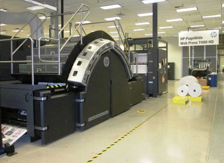
 HP Showcases PageWide Web Press HD in Corvallis HP Showcases PageWide Web Press HD in Corvallis
- The facility tour began with a visit to HP's Corvallis “Fab” lab, the fabrication laboratory where the silicon wafers used in inkjet print heads are made using micro electro mechanical system (MEMS) manufacturing techniques. The latest models use the ...
yesterday Printing Impressions (press release) - MEMS technology
 Is black phosphorous the next big thing in materials? Is black phosphorous the next big thing in materials?
- "The anisotropy we discovered in the thermal conductivity of black phosphorous nanoribbons indicates that when these layered materials are patterned into different shapes for microelectronic and optoelectronic devices, the lattice orientation of the ...
today EurekAlert (press release) - MEMS technology
 New Artificial Skin Is Sensitive to Touch and Feels Changes in Pressure New Artificial Skin Is Sensitive to Touch and Feels Changes in Pressure
- It's thin, flexible, made of organic material, and understands a range of pressures. Just like your fingertips. In fact, patches of this artificial skin already have been painted on mechanical hand-like prosthesis. A team led by Zhenan Bao, a chemical ...
yesterday Popular Mechanics - MEMS technology
MEMS business
 Large Inflow of Money Witnessed in KLA-Tencor Corporation Large Inflow of Money Witnessed in KLA-Tencor Corporation
- ... Reticle Manufacturing, Complementary Metal-Oxide-Semiconductor (CMOS) Image Sensors Manufacturing, Solar Manufacturing, light emitting diode (LED) Manufacturing, Data Storage Media/Head Manufacturing, Microelectromechanical Systems (MEMS) ...
yesterday Money Flow Index - MEMS business
 3D-PolySPRINT brings together eight companies to make 3D printed hearing aids ... 3D-PolySPRINT brings together eight companies to make 3D printed hearing aids ...
- LZH's Laser Micromachining Group is developing the necessary process, and focusing on multi-material 3D printing in order to achieve a hard inner core and comfortable, soft covering that will increase comfort and avoid unpleasant pressure sores ...
yesterday 3ders.org (blog) - MEMS business
 Theranos Isn't the Only One Chasing Needle-Free Blood Tests Theranos Isn't the Only One Chasing Needle-Free Blood Tests
- “One of the big challenges has been how you mix things in small volumes at a microscopic scale,” says Eugene Chan, microfluidics expert and head scientist at DNA Medical Institute in Cambridge, Massachusetts. Mixing pure liquids is hard enough, and it ...
today WIRED - MEMS business
 Saxony Leads Germany's Semis Saxony Leads Germany's Semis
- Electronic Design Chemnmitz, a spin-off company of the Chemnitz University of Technology and is located in the same industrial park as Fraunhaufer ENAS (Electronic Nano-system Institute) and specializes putting microelectromechanical systems (MEMS) ...
today EE Times - MEMS business
Nanotechnology
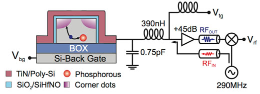
 Coupled quantum spins in a CMOS nano-device Coupled quantum spins in a CMOS nano-device
- These results are all the more important as they were observed in an electronic device made in an industrial microfabrication-compatible facility (situated in Grenoble, France). Silicon is a favoured material for making a scalable quantum computer ...
today Nanowerk - Nanotechnology
 Manipulating Graphene Oxide on the Nanoscale Manipulating Graphene Oxide on the Nanoscale
- According to the researchers, the 2-D nanomaterial has serious potential. “At first, this will mainly be useful for studying fundamental properties and lab-scale devices,” said Mativetsky. “Eventually, this work may help lead to the practical ...
2015-10-14 R & D Magazine - Nanotechnology
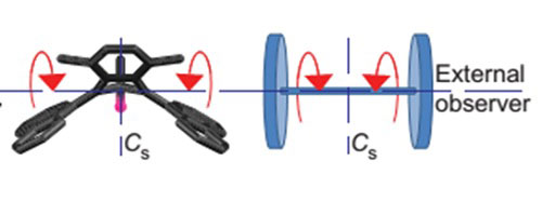
 New nanotechnology motor mimics two wheels on an axle New nanotechnology motor mimics two wheels on an axle
- (Nanowerk News) University of Groningen scientists led by Professor of Organic Chemistry Ben Feringa have designed a new type of molecular motor. In contrast to previous designs, this molecule is symmetrical. It comprises two parts, which are connected ...
yesterday Nanowerk - Nanotechnology
 Manipulating light at the nanoscale Manipulating light at the nanoscale
- Plasmonics is an enabling technology that incorporates noble metals to guide and manipulate light at optical frequencies on the surface of the metals. It allows the nanoscale confinement of light in gaps between two metal surfaces. This tight ...
2015-10-14 SPIE Newsroom - Nanotechnology
Featured Event
Attend SPIE Photonics West 2015, the #1 laser, photonics, and biomedical optics conference: 20,000 attendees, two exhibitions with more than 1,250 exhibiting companies, 70 special events, 4,800 papers in the areas of biomedical optics, optoelectronics, industrial lasers, nanophotonics, MOEMS-MEMs, and more. The Moscone Center, San Francisco, California, United States, 13 - 18 February 2016. Register today.
Event Calendar
- MicroTAS 2015
- 2015-10-25 - 2015-10-29
HICO, Gyeongju, Korea
The 19th International Conference on Miniaturized Systems for Chemistry and Life Sciences
|
|
- MEMS Executive Congress US 2015
- 2015-11-04 - 2015-11-06
Napa, CA
MEMS and Sensors: Enabling the Connection to the Physical World
|
|
- Wearable Sensors and Electronics 2015
- 2015-11-16 - 2015-11-17
Santa Clara, CA.
Bringing Together the Wearable Ecosystem
|
|
- PowerMEMS 2015
- 2015-12-01 - 2015-12-04
Boston, MA
The 15th International Conference on Micro and Nanotechnology Power Generation and Energy Conversion Applications
|
|
- T-Sensors Summit
- 2015-12-09 - 2015-12-10
Celebration, FL
Creating a TSensors-Based Abundant Future
|
|
- SPIE Photonics West 2016
- 2016-02-13 - 2016-02-18
Moscone Center San Francisco, California, USA
Photonics West, the #1 laser, photonics, biomedical optics conference
|
|
- MEMS Technical Congress Europe 2016
- 2016-03-07 - 2016-03-08
Munich, Germany
Delivering Technical Solutions, Together.
|
|
- MEMS 2017
- 2017-01-22 - 2017-01-26
Las Vegas, Nevada
The 30th Annual IEEE International Conference on Micro Electro Mechanical Systems
|
|
|
|