|
View Mailing Online
MEMS technology
 Advanced lithography and electroplating approach to form high-aspect ratio ... Advanced lithography and electroplating approach to form high-aspect ratio ...
- System Scaling Technology — the combination of front-end, middle-end and back-end to advance microelectronic systems—utilizes many different advanced packaging approaches, one of which is known as 2.5D packaging. The term “2.5D packaging” has ...
2015-12-08 ElectroIQ (blog) - MEMS technology
 None more black None more black
- It withstands launch shock, staging and long-term vibration, and is suitable for coating internal components, such as apertures, baffles, cold shields and Micro Electro Mechanical Systems (MEMS) –type optical sensors. “We are now scaling up production ...
yesterday Engineering Materials - MEMS technology
 Using microfluidics for tunable metamaterials Using microfluidics for tunable metamaterials
- In our RARM methodology (see Figure 1), we use microfluidic technology to create an array of microcavities that can be filled (in a controlled manner) with liquid metal. Our microfluidic network control system—see Figure 1(e)—is a purposely designed ...
yesterday SPIE Newsroom - MEMS technology
- Sony's handheld portable laser HD projector arrives Jan 2016
- The laser beam is then reflected and controlled using a MEMS (microelectromechanical systems) mirror to scan and project the image.' This processing system allows the MP-CL1 to project images at HD resolution and enables 'focus-free projection as well ...
yesterday iTWire - MEMS technology
MEMS business
 Chinese companies slotting into Taiwanese chipmaker's supply chain Chinese companies slotting into Taiwanese chipmaker's supply chain
- The Chinese companies include semiconductor materials makers Konfoong Materials International (KFMI) and Anji Microelectronics. Senior executives with Advanced Micro-Fabrication Equipment (AMEC), a Shanghai-based etching equipment manufacturer ...
2015-12-08 Nikkei Asian Review - MEMS business
 Often combining disciplines to innovate, UofL and UK scientists adance ... Often combining disciplines to innovate, UofL and UK scientists adance ...
- UofL built micro-electro-mechanical systems devices for the study in its Micro/Nano Technology Center at the Speed School. MEMS tend to be resistant to radiation conditions, and Alphenaar's three-year study will examine this. The devices are being ...
2015-12-08 The Lane Report - MEMS business
- MEMS pressure sensor industry attracts investors from different regions
- The MEMS Pressure Sensor Industry 2015 report provides a basic overview of the industry including definitions, classifications, applications and industry chain structure. The MEMS Pressure Sensor market analysis is provided for the international ...
yesterday WhaTech - MEMS business
- Orbotech Receives $57 Million in Orders From a Leading Semiconductor ...
- The company is a leading provider of yield enhancement and production solutions for electronics reading, writing and connecting, used by manufacturers of printed circuit boards, flat panel displays, advanced packaging, micro-electro-mechanical systems ...
yesterday PR Newswire (press release) - MEMS business
Nanotechnology
 Researchers develop nanoscale probes for ssDNA sustainability under UV radiation Researchers develop nanoscale probes for ssDNA sustainability under UV radiation
- DNA wrapped around nanotube (right inset) is capable to recover after absorbing ultraviolet (UV) radiation by an autoionization process. Experimental two-color fluorescence spectroscopy (left) was combined with quantum mechanical …more. DNA, which ...
2015-12-08 Phys.Org - Nanotechnology
 Researchers Develop New Method for Tracking the Motion of Nanoscale Viruses Researchers Develop New Method for Tracking the Motion of Nanoscale Viruses
- A novel technique that uses optical fibre to track the motion of a single virus has been developed. It is hoped that this technique will allow researchers to understand the mechanisms by which viruses multiply and accumulate.
today AZoNano - Nanotechnology
- New nanotechnology manufacturing technique advances imaging, biosensing technology
- (Nanowerk News) More than a decade ago, theorists predicted the possibility of a nanolens—a chain of three nanoscale spheres that would focus incoming light into a spot much smaller than possible with conventional microscopy. Such a device would make ...
yesterday Nanowerk - Nanotechnology
 Heat radiates 10000 times faster at the nanoscale Heat radiates 10000 times faster at the nanoscale
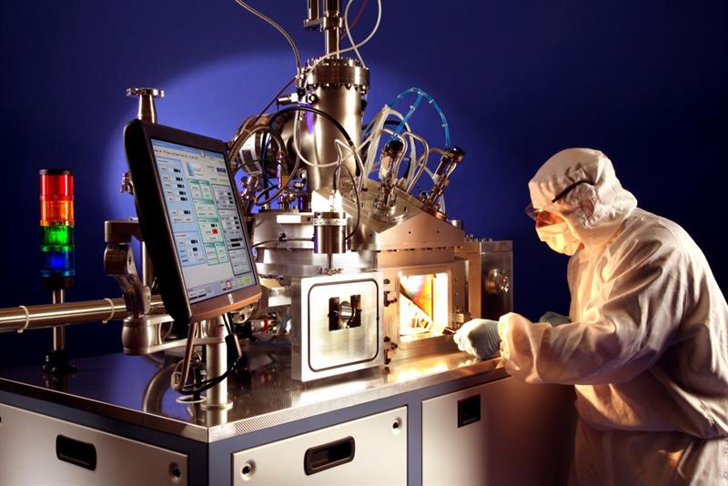
- The view inside the Ultra High Vacuum Scanning Thermal Microscope, which was used to measure temperature fluxes at the nanoscale. Credit: Joseph Xu. When heat travels between two objects that aren't touching, it flows differently at the smallest ...
today Phys.Org - Nanotechnology
Featured Event
Attend SPIE Photonics West 2015, the #1 laser, photonics, and biomedical optics conference: 20,000 attendees, two exhibitions with more than 1,250 exhibiting companies, 70 special events, 4,800 papers in the areas of biomedical optics, optoelectronics, industrial lasers, nanophotonics, MOEMS-MEMs, and more. The Moscone Center, San Francisco, California, United States, 13 - 18 February 2016. Register today.
Event Calendar
- SPIE Photonics West 2016
- 2016-02-13 - 2016-02-18
Moscone Center San Francisco, California, USA
Photonics West, the #1 laser, photonics, biomedical optics conference
|
|
- MEMS Technical Congress Europe 2016
- 2016-03-07 - 2016-03-08
Munich, Germany
Delivering Technical Solutions, Together.
|
|
- MEMS 2017
- 2017-01-22 - 2017-01-26
Las Vegas, Nevada
The 30th Annual IEEE International Conference on Micro Electro Mechanical Systems
|
|
|
|