|
View Mailing Online
MEMS technology
- Spies, military looking for hacker-, backdoor-proof circuits
- One type mentioned in its announcement are microelectromechanical systems, super-small chips that can be used to make things like very tiny advanced sensors. These kinds of chips have all kinds of military applications, helping to make 10-gram cameras ...
2011-06-24 Ars Technica - MEMS technology
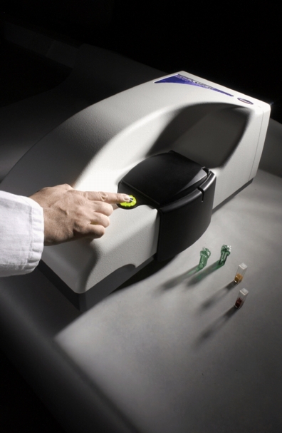
 Medical devices on fast forward Medical devices on fast forward
- Researchers plan to do this by using the burgeoning field of microfluidics — separating some substances from others, as a coin sorter splits nickels, dimes, and quarters. “At MIT we have arguably the most activity in microfluidics of any university in ...
yesterday Boston Globe - MEMS technology
 Texas Tech and Carnegie Mellon teams win at Sandia Labs MEMS competition Texas Tech and Carnegie Mellon teams win at Sandia Labs MEMS competition
- Travel funds provided by SPIE, the international society for optics and photonics, enabled greater participation by the universities, according to Sandia's Tom Zipperian, Senior Manager for MESA Microfabrication, and Keith Ortiz, Manager of MEMS ...
2011-06-24 SPIE Newsroom - MEMS technology
MEMS business
- Internationally recognized BME professor to join University of Texas as ...
- During his appointment at the BME Department, Khademhosseini will perform collaborative research with UT Austin faculty on merging microfabrication techniques and biomaterials for regenerative medicine and drug discovery applications. ...
today PhysOrg.com (press release) - MEMS business
- 3M Adds Temporary Wafer Bonding Application Lab in Taiwan
- Cambridge NanoTech Advances Nanotechnology With FijiTM Plasma ALD Systems. Posted: Jun 23rd, 2011. Lumerical's MODE Solutions 5.0-Broadband Omnidirectional Waveguide Design Tool. Posted: Jun 22nd, 2011 ...
today - MEMS business
- Elpida begins sample shipments of 3D-TSV stacked DDR3 DRAM
- Elpida Memory on June 27 announced that it has begun sample shipments of its DDR3 SDRAM (x32-bit I/O configuration) made using TSV stacking technology. The sample is a low-power 8Gb (1GB) DDR3 SDRAM assembled in a single package that consists of four ...
yesterday Digitimes - MEMS business
- Healthcare Applications for MEMS and BioMEMS , Medicine
- Micro system Devices Driving Healthcare Applications, Yole Development, Compound Semiconductor, Yole Development Services, Strategy & Technology Consulting Services, Publication of Market & Technology Reports, ...
2011-06-24 - MEMS business
 Movea unveils its Motionpods body motion capture system Movea unveils its Motionpods body motion capture system
- The micro-electromechanical system uses proprietary wireless technology instead of something like Bluetooth, mainly to keep power consumption low. The pods send their data to a USB device. Movea has also developed gesture recognition in the past and ...
today Inquirer - MEMS business
- Taking the Measure | Blogs on Test & Measurement World
- MEMS devices are becoming key components in the process of smart system ... Are RF MEMS devices commercially viable, or will they become so soon? ...
www.tmworld.com - MEMS business
- Yole new report on 3DIC & WLP Equipment and Materials
- For the first time, Yole's analysts have gathered all the necessary information to benchmark the different process alternatives required for wafer-level-packaging and 3DIC integration based on TSV interconnects.
yesterday Global SMT & Packaging Magazine - MEMS business
Nanotechnology
- Scientists pioneer nanoscale nuclear materials testing capability
- Scientists pioneer nanoscale nuclear materials testing capability.
today - Nanotechnology
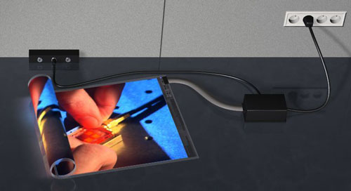
- Using a simple pen, you can literally write electronics on paper
- In a previous Nanotechnology Spotlight, we reported on an example of how researchers at the University of Illinois at Urbana-Champaign (UI) used this ink for the conformal printing of 3D electrically small antennas. ...
today - Nanotechnology
- Heidelberg Instruments to develop novel UColorado nanotechnology platform
- (Nanowerk News) A novel University of Colorado Boulder technique to shrink the size of circuitry used in nanotechnology devices like computer chips and solar cells by zapping a substrate with two separate colors of light beams has been optioned to ...
today Nanowerk LLC - Nanotechnology
- Organic electronics: Peel carefully
- Posted: Jun 24th, 2011. New nanotechnology knowledge transfer network "SafeNano Norway". Posted: Jun 24th, 2011. Obama calls for high-tech manufacturing effort involving nanotechnology. Posted: Jun 24th, 2011 ...
today - Nanotechnology
 SiMoNa optimizes organic light-emitting diodes SiMoNa optimizes organic light-emitting diodes
- Scientists of the KIT Institute of Nanotechnology (INT) have now developed a simulation method for the low-cost optimization of OLEDs within shorter time. By means of SiMoNa, material properties can be improved specifically and appropriate dye ...
today Nanowerk LLC - Nanotechnology
Nanotech business
 Malvern Zetasizer Nano shows aptitude for interdisciplinary research at Purdue Malvern Zetasizer Nano shows aptitude for interdisciplinary research at Purdue
- The system is housed within the Chemical Nanotechnology/Microfluidics laboratory and users range from those who are highly experienced with the instrument to complete novices. Lisa Reece is Lab Director of the IN-CTSI (Indiana-Clinical Translational ...
2011-06-25 Nanotechnology News (press release) - Nanotech business
 Hands-on courses prepare students for careers in nanotechnology Hands-on courses prepare students for careers in nanotechnology
- (Nanowerk News) Two million workers are projected to be needed in nanotechnology-based businesses by 2020 in the United States alone. Today, demand far outstrips the availability of trained personnel and the College of Engineering and Applied Science ...
today Nanowerk LLC - Nanotech business
 Malvern's Zetasizer Nano praised by Birck Nanotechnology Center Malvern's Zetasizer Nano praised by Birck Nanotechnology Center
- Malvern Instruments has won a recommendation for its Zetasizer Nano particle characterisation system from the Birck Nanotechnology Center (BNC). The research centre, which is located within the Discovery Park of Purdue University in Indiana, ...
today Zenopa - Nanotech business
Featured Process
MNX offers commercial e-beam lithography services using a state-of-the-art Vistec EBPG 5000+ direct-write tool. This affordable service provides you with the best performance and fastest turnaround times in the industry. | - 50MHz scan speed
- Spot size below 2.5 nm
- Large scan field size
- Fast cycle times
|
Event Calendar
|
|