|
View Mailing Online
MEMS technology
- Microlenses for 3D Endoscopes
- The ability to see inside the patient's body in perfect 3-D is the result of work by researchers at the Fraunhofer Institute for Microelectronic Circuits and Systems IMS in Duisburg and the project partners in the EU project "Minisurg". ...
today Product Design & Development - MEMS technology
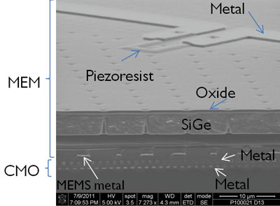
 Imec demonstrates CMOS integrated poly-SiGe piezoresistive pressure sensor Imec demonstrates CMOS integrated poly-SiGe piezoresistive pressure sensor
- This represents not only the first integrated poly-SiGe pressure sensor directly fabricated above its readout circuit, but also the first time that a poly-SiGe MEMS device is processed on top of Cu-backend CMOS. Polycrystalline SiGe has emerged as a ...
today Nanowerk LLC - MEMS technology
- MIT and ST co-develop low power SOC MPU
- An R&D project between the MTL (Microsystems Technology Laboratories) of Massachusetts Institute of Technology and STMicroelectronics has developed a reduced consumption 32-bit ultra-low-voltage microprocessor SOC which could be used in wireless ...
today EDN.com - MEMS technology
 Progress in quantum computing, qubit by qubit Progress in quantum computing, qubit by qubit
- "We've designed everything in parallel in a massive system, which allows us to make thousands or millions of devices with more or less the same properties, and we use conventional microfabrication and nanofabrication techniques, unlike what has been ...
today R & D Magazine - MEMS technology
 Power generated from human respiration? Power generated from human respiration?
- Also, PVDF being bio-compatible, the development shows a substantial advance in developing a micro-scale device for storing energy from respiration. The findings are published in the journal Energy and Environmental Science. ...
today HealthJockey.com - MEMS technology
MEMS business
- I-Micronews - ADVANCED PACKAGING: 3D IC, WLP & TSV ...
- “Pricing, especially for wide I/O memory stacks and high-density TSV interposers, and associated business models, are key challenges,'' Nowak said during a keynote at the International Wafer-Level Packaging Conference ...
2011-10-07 - MEMS business
- A Very iPad Christmas
- The MEMS display technology is alien to the rest of the market and superior for text presentation. Though still in its infancy, MEMS technology should eventually deliver the paper-perfect look that its supporters covet. So, no matter what else you own, ...
today PC Magazine - MEMS business
- IP Today-Should Scientists Boycott IP ...
- by Fundamentals of Microfabrication on October 8, 2011. I am very curious to find out what my scientist friends are thinking about Intellectual Property rights these days. Here are some observations that worry me: 1. As science collaborations ...
Fundamentals of Microfabrication 2011-10-08 - MEMS business
- Knowles Electronics Mems Joystick for Samsung Galaxy Tab ...
- With gaming on tablets, the visual experience is often top-notch, but the controls are unfamiliar at best -- even inadequate at times. But adding a.
Zach Honig 2011-10-07 - MEMS business
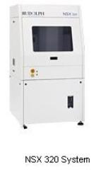
 Rudolph Delivers Wafer Scanner and Macro Defect Inspection Systems to ... Rudolph Delivers Wafer Scanner and Macro Defect Inspection Systems to ...
- The new NSX 320 System provides inspection solutions for the TSV-based processes to link numerous die in one package, while offering services to critical metrology and inspection solutions to sawn wafers on film frames, wafer-to-wafer arrangement in ...
2011-10-07 AZoNano.com - MEMS business
 Thin Wafer Market & Applications Thin Wafer Market & Applications
- CIS wafers will also be thinner for packaging purposes (TSV, WLCSP). Memories can be stacked in different ways: wire bonding or TSV. 3D stacking is the next big thing for memory integration with thickness as low as 25µ in 2016. ...
yesterday Global SMT & Packaging Magazine - MEMS business
- IQE Introduces Customisable Silicon on Insulator (SOI) With Improved Thickness ...
- These include advanced microprocessors, high-voltage devices and complex MEMs and sensors. The significant electrostatic benefits of replacing bulk silicon wafers with SOI include reduction of parasitic device capacitance and resistance to latch-up. ...
today Reuters (press release) - MEMS business
Nanotechnology
 Caltech Team Uses Laser Light to Cool Object to Quantum Ground State Caltech Team Uses Laser Light to Cool Object to Quantum Ground State
- By Caltech A scanning electron microscope image (a) of the nanoscale silicon mechanical resonator used in the laser cooling experiment. The outer “cross” patterning forms the shield while the central beam region, the SEM image of which is shown in (b), ...
today Product Design & Development - Nanotechnology
 The Nanotechnology of Sundew and English Ivy The Nanotechnology of Sundew and English Ivy
- This Behind the Scenes article was provided to LiveScience in partnership with the National Science Foundation. Fifteen small sundew plants perch on a windowsill collecting sunlight and eating meat in the lab of Mingjun Zhang on the University of ...
2011-10-07 LiveScience.com - Nanotechnology
- The Term 'Nanolargesse' Still Not in Common Usage
- While nanotechnology has not been a gold mine for creating new fortunes, it's certainly been one for “nano” being used as a prefix in quasi-portmanteaus as evidenced by the name of this blog and nearly every nano-related start-up company for the last ...
today IEEE Spectrum - Nanotechnology
- New Nanomaterial kills antibiotic-resistant bacteria
- A minster sches research team has developed a so far unique nanomaterial, the antibiotic-resistant bacteria kills. A minster sches research team has developed a so far unique nano-materials that are resistant to antibiotics kill ...
admin today - Nanotechnology
Nanotech business
- IBM's graphene nanoelectronics work wins ITRI's global ...
- IBM's graphene nanoelectronics work wins ITRI's global nanotechnology innovation contest. ... nanotechnology, nanotechnology links, nanomaterials, nanomaterial database, nanotechnology news. Click Here! ...
2011-10-07 - Nanotech business
- Research and Markets adds Report on Global Nanotechnology Market
- By Cameron Chai Research and Markets has added the report titled,The World Market For Nanotechnology: Nanomaterials, Markets and Companies 2011, to their offering. Nanomaterials and nanotechnology is a multi-billion dollar industry and experts predict ...
2011-10-07 AZoNano.com - Nanotech business
- Research and Markets Releases Report on Nanoscale Semiconductor-on-Insulator ...
- By Cameron Chai Online research website Research and Markets has released a report titled “Nanoscaled Semiconductor-on-Insulator Materials, Sensors and Devices”. The report was formulated from the papers submitted at the 6th International Workshop on ...
today AZoNano.com - Nanotech business
Featured Event
In its seventh year, MEMS Executive Congress is the executive conference that connects the MEMS supply chain with MEMS end-users. Through keynotes, panel discussions, and numerous networking opportunities, MEMS Executive Congress creates an intimate forum for decision-makers to grow the global MEMS market. Hosted by MEMS Industry Group (MIG).
Register Now!
Event Calendar
- Modeling and Simulation of Nano/Microsystems Contest
- 2011-08-29 - 2011-10-31
University of Michigan
|
|
- IMAPS 2011 - Microelectronics Symposium
- 2011-10-09 - 2011-10-13
Long Beach CA
Bringing Together The Entire Microelectronics Supply Chain!
|
|
- SENSORS Tech Forum '11 Boston
- 2011-10-10 - 2011-10-12
Boston, MA
NASA Tech Briefs Presents SENSORS Tech Forum
Visit MNX at this event
|
|
- MEMS in Motion Collaboration Summit
- 2011-10-12 - 2011-10-13
Palm Springs, CA
It's not who you know today. It's who you're going to need to know tomorrow.
Visit MNX at this event
|
|
- GSA Silicon Series
- 2011-10-20
Boston, MA
Investing in Motion: MEMS Inertial Sensors
|
|
- MEMS Testing and Reliability Conference
- 2011-10-20
Santa Clara CA
Increase yields, decrease waste and increase profitability for your company
|
|
- Technology Platform for Various MEMS Scanner Products
- 2011-10-20
Webinar - 11:30 AM ET, 8:30 AM PT
An Approach to Overcome MEMS Law
|
|
- MEMS Executive Congress 2011
- 2011-11-02 - 2011-11-03
Monterey, CA
Connecting the MEMS supply chain with MEMS end-users
Visit MNX at this event.
|
|
- American Manufacturing Strategies Summit 2011
- 2011-11-07 - 2011-11-08
Chicago IL
Network with 150 + senior level manufacturing professionals from many disciplines.
|
|
- 3-D Architectures for Semiconductor Integration and Packaging
- 2011-12-12 - 2011-12-14
Burlingame, California
Today's Manufacturing Advances, Tomorrow's Impact and Opportunity
|
|
- SPIE Photonics West 2012
- 2012-01-21 - 2012-01-26
San Francisco CA
The world's leading photonics, laser, and biomedical optics conference
|
|
- IEEE MEMS 2012
- 2012-01-29 - 2012-02-02
Paris, France
Focus on Strategies for Reducing Time and Cost of MEMS Testing
|
|
- MEMS Executive Congress 2012
- 2012-03-20
Zurich, Switzerland
MEMS Industry Group event co-located with Smart Systems Integration
|
|
- Hilton Head Workshop 2012
- 2012-06-03 - 2012-06-07
Hilton Head Island, SC
A Solid-State Sensors, Actuators and Microsystems Workshop
|
|
- Sensors Expo & Conference 2012
- 2012-06-06 - 2012-06-07
Rosemont (Chicago) IL
Providing over 25 Years of Technical Innovation & Thought Leadership
|
|
|
|