|
View Mailing Online
MEMS technology
 TSV inspection in 3D advanced packaging applications TSV inspection in 3D advanced packaging applications
- TSV nails are formed by filling vias, usually with copper, etched into the wafer. The wafer is then flipped and mounted to a carrier wafer. A combination of processes is used to remove material from the wafer surface, leaving the ends of the copper ...
today ElectroIQ - MEMS technology
 Photon management structures for solar cells Photon management structures for solar cells
- NIL describes a process sequence in which a polymer layer is first patterned by hot embossing or a UV-replication process, and this patterned layer is then used as an etching mask to transfer the defined patterns to a substrate underneath.
yesterday SPIE Newsroom - MEMS technology
 Microfluidic prototype has keys that rise out of the touchscreen Microfluidic prototype has keys that rise out of the touchscreen
- Demoed at Society for Information Display's Display Week 2012 and reported by The Verge, this microfluidic prototype display features a keyboard that can rise out of the panel when a user needs it and disappear once typing is no longer necessary.
today IntoMobile - MEMS technology
MEMS business
- Advantest Announces 3D TSV Stack Test Solutions
- By Business Wire By Bruce Armstrong Come to New York and get yourself up to date with the Big Data revolution! As advanced data storage, access and analytics technologies aimed at handling high-volume and/or fast moving data all move center stage, ...
yesterday SYS-CON Media (press release) - MEMS business
 UMC, IME team on TSV process for image sensors UMC, IME team on TSV process for image sensors
- The collaboration will make use of IME's 300-mm TSV production line which includes capabilities in TSV wafer thinning, wafer bonding, redistribution layer (RDL) and bumping. It is targeting improved sensitivity in smaller pixel image sensors.
today EE Times - MEMS business
- Schlumberger Launches Breakthrough Marine Seismic Technology
- The IsoMetrix system uses calibrated, multisensor MEMS technology that forms part of the new WesternGeco Nessie-6* point-receiver seismic streamer. The sensors measure acoustic pressure as well as vertical and crossline acceleration throughout the ...
yesterday MarketWatch (press release) - MEMS business
- Minnesota Telecom (NESC) Selects CALIENT and Cyan to Deploy the Industry's ...
- Cyan and CALIENT have built the industry's first colorless, directionless, contentionless (CDC) reconfigurable optical add-drop multiplexer (ROADM) using 3D MEMS photonic switching to deliver a cost-effective high add-drop ratio solution with complete ...
today MarketWatch (press release) - MEMS business
 MEMS processing unit completed at X-FAB silicon foundry in Germany HQ MEMS processing unit completed at X-FAB silicon foundry in Germany HQ
- June 4, 2012 -- X-FAB Silicon Foundries completed its dedicated noble metal facility for micro electro mechanical systems (MEMS) and post-complementary oxide metal semiconductor (CMOS) processing in Erfurt, Germany. The company also marked a milestone, ...
yesterday ElectroIQ - MEMS business
 Soldier-worn sensor that measures the destructive power of explosives uses ... Soldier-worn sensor that measures the destructive power of explosives uses ...
- Now the Analog Devices ADXL362 low-power accelerometer based on micro-electro-mechanical systems (MEMS) technology is planned for the second generation of DARPA's Blast Gauge. "The ADXL362 will significantly extend battery life in these sealed devices ...
yesterday Military & Aerospace Electronics - MEMS business
Nanotechnology
- Nanocones could be key to making inexpensive solar cells
- The hybrid solar cells' use of nanoscale texturing has two advantages: it improves light absorption and reduces the amount of silicon material needed. Previous nanoscale texturing of solar cells has involved nanowires, nanodomes, and other structures.
today Phys.Org - Nanotechnology
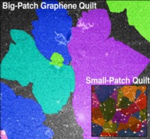
 Tighter 'stitching' means better graphene, say scientists Tighter 'stitching' means better graphene, say scientists
- The researchers, led by Jiwoong Park, assistant professor of chemistry and chemical biology and a member of the Kavli Institute at Cornell for Nanoscale Science, used advanced measurement and imaging techniques to make these claims, detailed online in ...
yesterday Nanotechnology News (press release) - Nanotechnology
 Bend me, shape me: flexible electronics perform under punishing conditions Bend me, shape me: flexible electronics perform under punishing conditions
- However, testing the durability of nanoscale electronics under strain—twisting, bending, folding, etc.—provides a challenge. The substrate (the layer upon which electronic components are assembled) and the electronics must endure stresses, ...
today Ars Technica - Nanotechnology
Featured Event
The AVS 59th International Symposium and Exhibition will be held October 28-November 2, 2012, at the Tampa Convention Center in Tampa, Florida. Highlights include an extensive collection of technical sessions, exhibitor technology spotlights, short courses, and a free to attend equipment exhibition.
Event Calendar
- Design Automation Conference (DAC) 2012
- 2012-06-03 - 2012-06-07
San Francisco CA
|
|
- Hilton Head Workshop 2012
- 2012-06-03 - 2012-06-07
Hilton Head Island, SC
A Solid-State Sensors, Actuators and Microsystems Workshop
Visit MNX at this event.
|
|
- Sensors Expo & Conference 2012
- 2012-06-06 - 2012-06-07
Rosemont (Chicago) IL
Providing over 25 Years of Technical Innovation & Thought Leadership
|
|
- Innovative MEMS Packaging for Future Technologies
- 2012-06-13
Online 11:30 AM ET, 8:30 AM PT
Presented by Andrew Oliver, PhD, WIMS2 Univ of Michigan
|
|
- IMS 2012 International Microwave Symposium
- 2012-06-17 - 2012-06-22
Montreal Canada
Celebrate the 60th anniversary of both the Microwave Theory and Techniques Society and the International Microwave Symposium
|
|
- ACTUATOR 2012
- 2012-06-18 - 2012-06-20
Bremen, Germany
International Conference and Exhibition on New Actuators and Drive Systems
|
|
- TechConnect World Summit & Innovation Showcase
- 2012-06-18 - 2012-06-21
Santa Clara CA
Increase your Innovation Pipeline!
|
|
- SEMICON West 2012
- 2012-07-10 - 2012-07-12
San Francisco CA
Connect to Buyers, Grow your Business!
|
|
- 45th Int'l Symposium on Microelectronics
- 2012-09-09 - 2012-09-13
San Diego CA
Bringing Together The Entire Microelectronics Supply Chain!
|
|
- MEMS in Motion Collaboration Summit
- 2012-09-12 - 2012-09-13
Palm Springs, CA
Collaboration & Networking on Steroids!
|
|
- AVS 59th International Symposium and Exhibition
- 2012-10-28 - 2012-11-02
Tampa Florida
|
|
- MEMS Executive Congress US 2012
- 2012-11-07 - 2012-11-08
Scottsdale AZ
|
|
- PowerMEMS 2012
- 2012-12-02 - 2012-12-05
Atlanta, Georgia
The 12th International Workshop on Micro and Nanotechnology for Power Generation and Energy Conversion Applications
|
|
- SPIE Photonics West 2013
- 2013-02-02 - 2013-02-07
San Francisco CA
The Conference and Marketplace for the Photonics, Biophotonics, and Laser Industry
|
|
- SPIE Advanced Lithography 2013
- 2013-02-24 - 2013-02-28
San Jose, CA
The world's premier semiconductor lithography conference and exhibition
|
|
|
|