|
View Mailing Online
MEMS technology
- SUSS coating/developing platform suits MEMS, packaging, LED fab, more
- SUSS MicroTec uncrated the third generation of the ACS200 Coating and Developing Platform, developed from the company's ACS200Plus and Gamma platforms for a compact, highly precise MEMS, LED, and related fab tool.
today ElectroIQ - MEMS technology
- Omron to Debut MEMS Absolute Pressure Sensor
- Omron will be exhibiting its new MEMS absolute pressure sensor at the Micromachine/MEMS ROBOTECH 2012 exhibition at Tokyo Big Sight from July 11 (Wed) to July 13 (Fri). As described by the company, the features include: 1. Subminiature dimensions ...
yesterday ElectroIQ - MEMS technology
- New Thermoreflectance Image Analyzer
- The TIA systems are based on the optical thermoreflectance principle coupled with digital signal processing and advanced patented software algorithms to support microelectronic component thermal characterization for thermal design validation, defect ...
today Sacramento Bee - MEMS technology
 InvenSense claims smallest 6-axis MEMS combo sensor InvenSense claims smallest 6-axis MEMS combo sensor
- The single-chip design combines a micro electro mechanical system (MEMS) 3-axis gyroscope and 3-axis accelerometer with an onboard Digital Motion Processor (DMP). The MPU-6500 MotionTracking device offers nearly 60% lower power (1.8V operation) ...
today ElectroIQ - MEMS technology
 Nordson's Plasma System Lowers Handling Risk to Sensitive Substrate Materials Nordson's Plasma System Lowers Handling Risk to Sensitive Substrate Materials
- Nordson MARCH has launched the new FasTRAK Plasma System, which is a high-throughput, fully-automated, vacuum plasma treatment system developed for laminate substrates, lead-frame strips, and other strip-type microelectronic components.
today Azom.com - MEMS technology
 MEMS microphones in plastic MEMS microphones in plastic
- STMicroelectronics has commenced mass production of MEMS microphones in plastic packages. The patented technology breakthrough saves space and increases durability in consumer and professional voice-input applications, from mobile phones and ...
yesterday Dataweek (press release) - MEMS technology
MEMS business
- EV Group's GEMINI® Wafer Bonding System First to Pass Equipment Maturity ...
- "EVG is the first company to pass ISMI's Equipment Maturity Assessment methodology," said Sitaram Arkalgud, director of SEMATECH's 3D Interconnect program. "3D is a major industry transition, and SEMATECH's 3D program members and supplier ...
today MarketWatch (press release) - MEMS business
- Silex Microsystems Receives VINNOVA Grant to Expand Volume Production ...
- JARFALLA, Sweden, July 9, 2012 /PRNewswire via COMTEX/ -- Silex Microsystems, the world's largest pure-play MEMS foundry, today announced that VINNOVA, the Swedish Governmental Agency for Innovation Systems, has awarded a nearly 10M SEK ...
yesterday MarketWatch (press release) - MEMS business
Nanotechnology
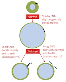
 Tiny bubbles snap carbon nanotubes like twigs Tiny bubbles snap carbon nanotubes like twigs
- “We find that the old saying 'I will break but not bend' does not hold at the micro- and nanoscale,” said Rice engineering researcher Matteo Pasquali, the lead scientist on the study, which appears this month in the Proceedings of the National Academy ...
yesterday ScienceBlog.com (blog) - Nanotechnology
 Nanotechnology set to technologically revolutionise sport Nanotechnology set to technologically revolutionise sport
- Advances in nanotechnology, '3D printing' and biomedical engineering are set to bring about a technological revolution in sport over the next few years, according to a new report launched by the Institution of Mechanical Engineers (IMechE).
today Engineering Capacity - Nanotechnology
- Scientists 'fingerprint' nanoscale objects and viruses
- Spanish scientists at the University of Barcelona have found a way of effectively identifying nanoscale objects and viruses that could offer a breakthrough for biomedical diagnostics, environmental protection and nano-electronics.
yesterday Phys.Org - Nanotechnology
 White LEDs Directly on Paper White LEDs Directly on Paper
- Gul Amin, who recently received his doctorate at the Physical Electronics and Nanotechnology group, Campus Norrköping, shows in his thesis how it is possible to grow white LEDs, made from zinc oxide and a conducting polymer, directly on a piece of paper.
today Product Design & Development - Nanotechnology
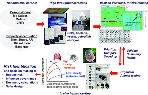
 Towards high-throughput, mechanisms-based toxicity testing of nanomaterials Towards high-throughput, mechanisms-based toxicity testing of nanomaterials
- Towards high-throughput, mechanisms-based toxicity testing of nanomaterials.
yesterday Nanowerk LLC - Nanotechnology
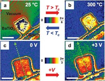
 Scientists Image Individual Atoms of Ferroelectric Nanomaterials Scientists Image Individual Atoms of Ferroelectric Nanomaterials
- Ferroelectric materials can store digital information just like their cousins, the ferromagnetic materials. Similar to the ferromagnetic materials being characterized by magnetic dipoles of either north or south and their capability to align themselves ...
yesterday AZoNano.com - Nanotechnology
 Picometer-precision imaging of electrical fields reveals mysteries of ... Picometer-precision imaging of electrical fields reveals mysteries of ...
- Brookhaven National Laboratory scientists recently used a technique called electron holography to capture images of the electric fields created by atomic displacement in exotic ferroelectric materials. The technique can resolve to the picometer scale ...
yesterday R & D Magazine - Nanotechnology
Nanotech business
- 'It's about achievement'
- The fast-growing College of Nanoscale Science and Engineering, now in yet another construction phase on the northwestern edge of the University at Albany campus, is considered the nation's premier research facility for nanotechnology, and Kaloyeros has ...
yesterday Albany Times Union - Nanotech business
Featured Event
The AVS 59th International Symposium and Exhibition will be held October 28-November 2, 2012, at the Tampa Convention Center in Tampa, Florida. Highlights include an extensive collection of technical sessions, exhibitor technology spotlights, short courses, and a free to attend equipment exhibition.
Event Calendar
- SEMICON West 2012
- 2012-07-10 - 2012-07-12
San Francisco CA
Connect to Buyers, Grow your Business!
|
|
- MEMS: Looking for the Next Killer App
- 2012-07-25
Webinar: 11:30 AM ET, 8:30 AM PT
|
|
- 45th Int'l Symposium on Microelectronics
- 2012-09-09 - 2012-09-13
San Diego CA
Bringing Together The Entire Microelectronics Supply Chain!
|
|
- Healthcare is Brimming with Opportunities for MEMS
- 2012-09-11
Webinar: 11:30 AM ET, 8:30 AM PT
|
|
- MEMS in Motion Collaboration Summit
- 2012-09-12 - 2012-09-13
Palm Springs, CA
Collaboration & Networking on Steroids!
|
|
- MIG Workshop at BSAC Fall 2012 Conference
- 2012-09-19 - 2012-09-21
UC Berkeley, CA
MEMS Product Development Challenges - Sweet Dreams and Nightmares
|
|
- 3rd Annual American Manufacturing Strategies Summit 2012
- 2012-10-22 - 2012-10-24
Chicago, IL
The stage is set for the 3rd American Manufacturing Strategies Summit 2012 in Chicago
|
|
- AVS 59th International Symposium and Exhibition
- 2012-10-28 - 2012-11-02
Tampa Florida
|
|
- MEMS Executive Congress US 2012
- 2012-11-07 - 2012-11-08
Scottsdale AZ
|
|
- PowerMEMS 2012
- 2012-12-02 - 2012-12-05
Atlanta, Georgia
The 12th International Workshop on Micro and Nanotechnology for Power Generation and Energy Conversion Applications
|
|
- SPIE Photonics West 2013
- 2013-02-02 - 2013-02-07
San Francisco CA
The Conference and Marketplace for the Photonics, Biophotonics, and Laser Industry
|
|
- SPIE Advanced Lithography 2013
- 2013-02-24 - 2013-02-28
San Jose, CA
The world's premier semiconductor lithography conference and exhibition
|
|
|
|