|
View Mailing Online
MEMS technology
- X-Fab has open platform MEMS 3D inertial sensor process for prototyping
- X-Fab has an open-platform MEMS 3D inertial sensor process available for engineering services and early access prototyping, with full qualification and complete design rule access coming early in 2013. Customers can run their own designs on the process ...
yesterday ElectronicsWeekly.com - MEMS technology
- DARPA taps NG on MEMS inertial sensors
- Under the Defense Advanced Research Projects Agency (DARPA) Primary and Secondary Calibration on Active Layer (PASCAL) effort of the Micro-Technology for Positioning, Navigation and Timing (Micro-PNT) programme, Northrop Grumman and the ...
today Air Traffic Management - MEMS technology
MEMS business
- Allegro and UMC Establish Foundry Partnership
- Allegro MicroSystems, Inc. is a leader in developing, manufacturing and marketing high-performance semiconductors. Allegro's innovative solutions serve high-growth applications within the automotive market, with additional focus on office automation, ...
2012-09-21 MarketWatch (press release) - MEMS business
- Mobile Device Sensor Market Worth $1.2 Billion at End of 2012, Says ABI ...
- LONDON — The ever growing popularity of mobile devices and increasing usage of MEMS sensors are set to drive sales for MEMS sensor vendors. New market intelligence from ABI Research projects the MEMS sensor market in mobile devices will be ...
2012-09-21 The Herald | HeraldOnline.com - MEMS business
 Will 3D Printing Save The 'TechBelt'? Will 3D Printing Save The 'TechBelt'?
- ExOne, an additive manufacturing and micromachining company based out of North Huntingon, Penn., is one of the handful of private companies — along with universities and other public institutions — to work together on the NAMII proposal, and is now ...
today Manufacturing.net - MEMS business
Nanotechnology
- New step to produce nanotechnology biosensors for cancer diagnosis
- New step to produce nanotechnology biosensors for cancer diagnosis. (Nanowerk News) Researchers from Shiraz University succeeded in the identification of presence or absence of any of the spot jumps in DNA sequence by designing a method that ...
today Nanowerk LLC - Nanotechnology
 New Stamping Process to Produce Precise Biomolecular Structures at Nanoscale New Stamping Process to Produce Precise Biomolecular Structures at Nanoscale
- Reactive stamps remove molecules from surfaces to create precise nanoscale patterns. Researchers from UCLA have reversed this traditional "soft lithography" process in order to address this problem. They utilized stamps that were chemically treated, ...
today AZoNano.com - Nanotechnology
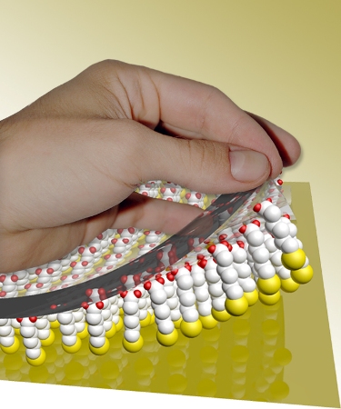
 Researchers demonstrate “giant” forces in super-strong nanomaterials Researchers demonstrate “giant” forces in super-strong nanomaterials
- They add that their finding "will open the door for various optomechanical applications in nanoscale, such as optical nanoelectromechanical systems, optical sensors and actuators." By experimenting with materials at the nanometer level, researchers ...
today R & D Magazine - Nanotechnology
 Nanotechnology could produce glass that's about twice as strong as the best ... Nanotechnology could produce glass that's about twice as strong as the best ...
- But scientists who look at the structure of glass strictly by the numbers believe some of the latest methods from the microelectronics and nanotechnology industry could produce glass that's about twice as strong as the best available today. Rice ...
today Nanowerk LLC - Nanotechnology
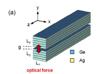
 New Nanoscale Slot Waveguides Exhibit Stronger Transverse Optical Force New Nanoscale Slot Waveguides Exhibit Stronger Transverse Optical Force
- By Will Soutter. In a research article that appeared in Optics Express, Drs. Xiaodong Yang and Jie Gao, scientists at Missouri University of Science and Technology, have described a new range of nanoscale slot waveguides that pack 100-1000 folds more ...
today AZoNano.com - Nanotechnology
- Researchers devise new 'subtractive' type of nanoscale printing
- (Phys.org)—The normal process for printing is centuries old, a piece of material such as wood is fashioned to look like the desired output, a letter of the alphabet, for example resulting in a stamp. Ink is then applied to the ...
2012-09-21 - Nanotechnology
Nanotech business
- Report on the Indian Nanotechnology Market
- Market research solutions provider, Research and Markets, has published a new report titled, "Nanotechnology Market in India 2012 – Update.” Nanotechnology refers to that realm of nanoscience that deals with not only applications of nanoscience but ...
yesterday AZoNano.com - Nanotech business
Featured Event
The AVS 59th International Symposium and Exhibition will be held October 28-November 2, 2012, at the Tampa Convention Center in Tampa, Florida. Highlights include an extensive collection of technical sessions, exhibitor technology spotlights, short courses, and a free to attend equipment exhibition.
Event Calendar
- 2012 Status of the MEMS Industry
- 2012-10-03
Webinar: 11:30 AM ET, 8:30 AM PT
Presented by: Dr Eric Mounier, Senior Analyst, MEMS Devices & Technologies, Yole Developpement
|
|
- Microfluidics 2012
- 2012-10-17
Santa Clara, CA
1st Annual Conference on Microfluidic Technologies and Applications
|
|
- MEMS Testing and Reliability 2012
- 2012-10-18
Santa Clara, CA
4th Annual Conference on MEMS Testing and Reliability
|
|
- 3rd Annual American Manufacturing Strategies Summit 2012
- 2012-10-22 - 2012-10-24
Chicago, IL
The stage is set for the 3rd American Manufacturing Strategies Summit 2012 in Chicago
|
|
- AVS 59th International Symposium and Exhibition
- 2012-10-28 - 2012-11-02
Tampa Florida
|
|
- MEMS Executive Congress US 2012
- 2012-11-07 - 2012-11-08
Scottsdale AZ
|
|
- PowerMEMS 2012
- 2012-12-02 - 2012-12-05
Atlanta, Georgia
The 12th International Workshop on Micro and Nanotechnology for Power Generation and Energy Conversion Applications
|
|
- MEMS in Medical Devices
- 2012-12-03 - 2012-12-03
San Jose, CA
|
|
- 3-D Architectures for Semiconductor Integration and Packaging Conference
- 2012-12-12 - 2012-12-14
Sofitel San Francisco Bay, Redwood City, CA
|
|
- MEMS TechZone and Conference Session at 2013 International CES
- 2013-01-08 - 2013-01-11
Las Vegas, Nevada
LVCC, South Hall 2, Booth 25321
|
|
- SPIE Photonics West 2013
- 2013-02-02 - 2013-02-07
San Francisco CA
The Conference and Marketplace for the Photonics, Biophotonics, and Laser Industry
|
|
- SPIE Advanced Lithography 2013
- 2013-02-24 - 2013-02-28
San Jose, CA
The world's premier semiconductor lithography conference and exhibition
|
|
- MicroManufacturing Conference & Exhibits
- 2013-04-16 - 2013-04-17
Hilton Minneapolis, MN
|
|
|
|