|
View Mailing Online
MEMS technology
 Copper, gold and tin for efficient chips Copper, gold and tin for efficient chips
- (Nanowerk News) With gold, copper or tin and special galvanizing processes, scientists are improving the function of semi-conductors and making the manufacture of microelectronic systems a child's play. Especially the LED industry could profit from this.
today Nanowerk LLC - MEMS technology
 Thermographic Evaluation of Forced Convective Heat Transfer Coefficient at ... Thermographic Evaluation of Forced Convective Heat Transfer Coefficient at ...
- Improved heat transfer surfaces with short pin fins are often used in various engineering fields such as in gas turbine blades cooling and in microelectronic applications. In these applications, the most widely utilized cooling element is the air ...
today Azom.com - MEMS technology
- Curved LCD could be used for displays in contact lenses
- The new display was produced at the Centre of Microsystems Technology (CMST), the associated laboratory of Interuniversity Microelectronics Centre (IMEC), at Ghent University. The video below shows off the new contact lens display with the ...
today Gizmag - MEMS technology
MEMS business
 Qualcomm and Sharp: MEMS and IGZO Tie the Knot Qualcomm and Sharp: MEMS and IGZO Tie the Knot
- Qualcomm subsidiary Pixtronix, has developed a microelectromechanical system ( MEMS ) Digital Micro Shutter (DMS) which is a low-power alternative to the liquid crystals used to create images in liquid crystal displays (LCDs). According to EE Times ...
yesterday NASDAQ - MEMS business
- MEMS Industry Group Showcases MEMS and the Consumer Experience at 2013 ...
- PITTSBURGH, Dec 06, 2012 (BUSINESS WIRE) -- MEMS Industry Group (MIG), a global industry organization with more than 150 member-companies and partners, today announced a micro-electromechanical systems (MEMS) conference track at the 2013 ...
today MarketWatch (press release) - MEMS business
 KLA-Tencor's updated LED wafer inspection tool boosts throughput, efficiency KLA-Tencor's updated LED wafer inspection tool boosts throughput, efficiency
- December 6, 2012 - KLA-Tencor says its new fourth-generation LED wafer inspection system achieves greater flexibility, increased throughput, and improved efficiency for inspecting defects and performing 2D metrology in LED applications, as well as MEMS ...
today ElectroIQ - MEMS business
 MEMS in Military and Aerospace Apps to Grow MEMS in Military and Aerospace Apps to Grow
- The microelectromechanical systems (MEMS) market for pressure sensors in the high-value military and aerospace segments will enjoy brisk double-digit growth this year, with plenty of room left for future expansion in a broad range of lucrative ...
today Novus Light Technologies Today - MEMS business
Nanotechnology
 Look Inside a Futuristic Nanotech Lab Look Inside a Futuristic Nanotech Lab
- College of Nanoscale Science and Engineering at SUNY Albany. December 6, 2012 12:21 PM Text Size: A . A . A. Physicist Richard Feynman famously said that there's plenty of room at the bottom. Room to build complex structures, machines, and computing ...
today Popular Mechanics - Nanotechnology
- Seeing in color at the nanoscale
- If nanoscience were television, we'd be in the 1950s. Although scientists can make and manipulate nanoscale objects with increasingly awesome control, they are limited to black-and-white imagery for examining those objects. Information about nanoscale ...
today Phys.Org - Nanotechnology
 Nanolithography for Fabricating Chiral Nanostructures Nanolithography for Fabricating Chiral Nanostructures
- This use of this technique is reported in a recent article published in the Advanced Optical Materials section of Advanced materials: "Circular Dichroism from Chiral Nanomaterial Fabricated by On-Edge Lithography". Simulations and optical-transmission ...
today Nanotechnology News (press release) - Nanotechnology
 WF Nanotechnology Center Develops Nearly Indestructible Molded Plastic Lights WF Nanotechnology Center Develops Nearly Indestructible Molded Plastic Lights
- “These lights are nearly indestructible and last an incredibly long time,” said David Carroll, Director of the Center for Nanotechnology and Molecular Materials at Wake Forest where the new lighting technology was developed. “I've had one going in the ...
today AZoNano.com - Nanotechnology
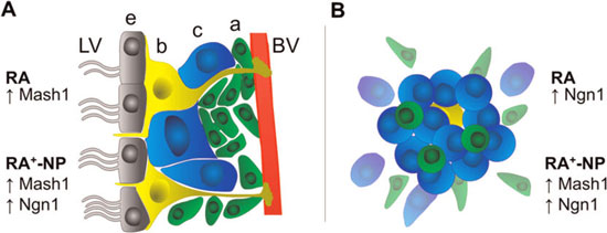
 Nanoparticles to control the differentiation of neural stem cells inside the brain Nanoparticles to control the differentiation of neural stem cells inside the brain
- Neuroscientists and cell biologists are keen to use nanotechnologies to manipulate endogenous stem cell niches such as the SVZ. New work, published in the November 23, 2012 online edition of ACS Nano ("Polymeric Nanoparticles to Control the ...
today Nanowerk LLC - Nanotechnology
Nanotech business
- Arsenal Improves High-Throughput Slit-Surface Electrospinning Technology for ...
- ... has shown that its processing technology can increase the manufacturing rates of core-sheath fibers (concentrically layered nano- or micro-scale fibers) more than 400 fold, compared with current state-of-the-art needle-based electrospinning techniques.
today AZoNano.com - Nanotech business
- Lockheed Martin partners LCN for nanotechnology research
- (Nanowerk News) A new research partnership, for the joint research and development of quantum and nanotechnologies, has been launched today between Lockheed Martin and the London Centre for Nanotechnology (LCN) at University College London ...
today Nanowerk LLC - Nanotech business
Featured Event
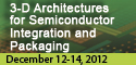
The 9th international conference, 3-D Architectures for Semiconductor Integration and Packaging, brings together technology and business leaders from around the world to take a look at the technology and market landscape for emerging 3-D device and systems integration and interconnect. Today, questions around 3-D solutions increasingly focus on when, not if, the industry will see product introduction and high volume manufacturing. Products based on 3-D chip scale packaging have already made significant inroads, in particular for image sensors, and 2.5-D devices with interposers, e.g. in FPGAs, are also seeing market introduction, and very healthy market growth for such uses is widely anticipated. Register now at techventure.rti.org. Event Calendar
- 3-D Architectures for Semiconductor Integration and Packaging Conference
- 2012-12-12 - 2012-12-14
Sofitel San Francisco Bay, Redwood City, CA
|
|
- MEMS TechZone and Conference Session at 2013 International CES
- 2013-01-08 - 2013-01-11
Las Vegas, Nevada
LVCC, South Hall 2, Booth 25321
|
|
- SPIE Photonics West 2013
- 2013-02-02 - 2013-02-07
San Francisco CA
The Conference and Marketplace for the Photonics, Biophotonics, and Laser Industry
|
|
- SPIE Advanced Lithography 2013
- 2013-02-24 - 2013-02-28
San Jose, CA
The world's premier semiconductor lithography conference and exhibition
|
|
- BioMedical MEMS and Sensors 2013
- 2013-04-16 - 2013-04-18
Cleveland, OH
MEMS technologies for biomedical applications
|
|
- MicroManufacturing Conference & Exhibits
- 2013-04-16 - 2013-04-17
Hilton Minneapolis, MN
|
|
- Nanotech Conference & Expo
- 2013-05-12 - 2013-05-15
Washington DC
|
|
- Design Automation Conference (DAC) 2013
- 2013-06-02 - 2013-06-06
Austin, Texas
Celebrating 50 Years !
|
|
- Sensors Expo and Conference
- 2013-06-05 - 2013-06-06
Rosemont, IL
Sensing Technologies Driving Tomorrow's Solutions
|
|
|
|
.jpg)