|
View Mailing Online
MEMS technology
 World's most sensitive plasmon resonance sensor inspired by ancient Roman cup World's most sensitive plasmon resonance sensor inspired by ancient Roman cup
- “It can be used for chemical imaging, biomolecular imaging, and integration to portable microfluidics devices for lab-on-chip-applications. His research team's results were featured in the cover article of the inaugural edition of Advanced Optical ...
today R & D Magazine - MEMS technology
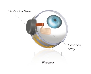
 FDA Approves First Retinal Implant FDA Approves First Retinal Implant
- The company's technology is a three- by three-millimeter microelectronic chip (0.1-millimeter thick) containing about 1,500 light-sensitive photodiodes, amplifiers and electrodes surgically inserted beneath the fovea (which contains the cone cells) in ...
today Nature.com - MEMS technology
 The Rise (or Fall?) of the Tactus Keyboard The Rise (or Fall?) of the Tactus Keyboard
- Tactus, using it's “microfluidics” technology, would be smart enough to sprout physical buttons from your screen, just for the duration of input. As the device nears the market–2013 is meant to be the year Tactus enters production, reportedly–CNET goes ...
yesterday MIT Technology Review - MEMS technology
 Darpa Wants Teeny-Tiny Fluids to Cool Down Next-Gen Microchips Darpa Wants Teeny-Tiny Fluids to Cool Down Next-Gen Microchips
- Darpa's plan: embed them with tiny fluid channels to circulate really, really small blobs of water. This month, the agency released a solicitation asking the industry to come up with designs for “microfluidic” cooling systems which can be embedded into ...
today Wired - MEMS technology
MEMS business
- Digital Speaker Development Update
- Audio Pixels patented technologies employ entirely new techniques to generate sound waves directly from a digital audio stream using low cost micro-electromechanical structures (MEMS) rather than conventional loudspeaker elements. This innovation ...
today Sacramento Bee - MEMS business
 Laird Technologies Acquires Nextreme Thermal Solutions Technology Laird Technologies Acquires Nextreme Thermal Solutions Technology
- Micro-scale form factors, high power-pumping capabilities and a high-volume semiconductor manufacturing process enables low-cost, high-performance thermal management and energy harvesting solutions. For more information, visit www.nextreme.com .
today ThomasNet Industrial News Room (press release) - MEMS business
Nanotechnology
 Nanotechnology in Organic Photovoltaics Nanotechnology in Organic Photovoltaics
- Developing clean alternatives to nuclear and fossil energy is essential for the growth of sustainable economies. One of the most attractive alternatives is photovoltaic (PV) technology, using the almost limitless power of the sun to generate electricity.
today AZoNano.com - Nanotechnology
 Nanosensors support skin cancer therapy Nanosensors support skin cancer therapy
- The work was supported by the NanoTera project "Probe Array Technology for Life Science Applications" of the Swiss National Science Foundation, by the Swiss Nanoscience Institute, the Cleven foundation and the microfabrication division of IBM Research ...
yesterday Nanowerk LLC - Nanotechnology
 New Nanoscale Engine to Generate Electricity from Waste Using Quantum Dots New Nanoscale Engine to Generate Electricity from Waste Using Quantum Dots
- A new type of nanoscale engine has been proposed that would use quantum dots to generate electricity from waste heat, potentially making microcircuits more efficient. An array on nano energy harvesters in what the researchers call a "swiss cheese" ...
yesterday AZoNano.com - Nanotechnology
Nanotech business
 Collaborative effort to advance NEMS switch technology for ultra low power ... Collaborative effort to advance NEMS switch technology for ultra low power ...
- (Nanowerk News) A*STAR's Institute of Microelectronics (IME) and Stanford University will collaborate to advance innovations in nano-electromechanical systems (NEMS) switch technology for ultra low power digital systems. The use of NEMS switches in ...
today Nanowerk LLC - Nanotech business
- Christine Peterson Looks into the Future of Nanotechnology
- I ran afoul of the Foresight Institute in my very first blog post here on the Spectrum website. The fiery response that post received from one of its members really should have come as no surprise to me based on the religious-like fervor Foresight ...
today IEEE Spectrum - Nanotech business
Featured Event
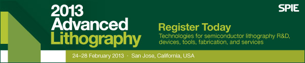
Advanced Lithography 2013 features the latest research and technological advancements in semiconductor lithography including: advanced etch technology and nanopatterning; extreme ultraviolet lithography; metrology; inspection and process control for microlithography; advances in resist materials and processing technology; and optical microlithography. The conferences and exhibition will be held in San Jose, California, 24-28 February 2013.
Event Calendar
- SPIE Advanced Lithography 2013
- 2013-02-24 - 2013-02-28
San Jose, CA
The world's premier semiconductor lithography conference and exhibition
|
|
- MIG MEMS Executive Congress Europe 2013
- 2013-03-12
Amsterdam, The Netherlands
Co-located with Smart Systems Integration 2013
|
|
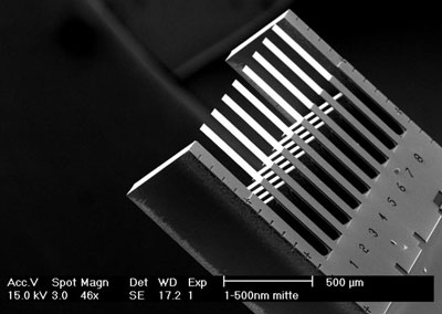
- Inertial Micropump Technology for Microfluidic Applications
- 2013-03-27
Online 11:30 AM ET, 8:30 AM PT
|
|
- BioMedical MEMS and Sensors 2013
- 2013-04-16 - 2013-04-18
Cleveland, OH
MEMS technologies for biomedical applications
|
|
- MicroManufacturing Conference & Exhibits
- 2013-04-16 - 2013-04-17
Hilton Minneapolis, MN
|
|
- MIG M2M Forum
- 2013-05-08 - 2013-05-09
Boston, MA
The annual members' meeting of MEMS Industry Group.
|
|
- Nanotech Conference & Expo
- 2013-05-12 - 2013-05-15
Washington DC
|
|
- Mid-Atlantic Micro/Nano Alliance Spring Symposium
- 2013-05-14
NIST, Gaithersburg MD
"Microsystems Technology: Fulfilling the Promise"
|
|
- Design Automation Conference (DAC) 2013
- 2013-06-02 - 2013-06-06
Austin, Texas
Celebrating 50 Years !
|
|
- International Microwave Symposium (IMS)
- 2013-06-02 - 2013-06-07
Seattle, Washington
Join top engineers and scientists in the RF & Microwave Field at IMS!
|
|
- Sensors Expo and Conference
- 2013-06-05 - 2013-06-06
Rosemont, IL
Sensing Technologies Driving Tomorrow's Solutions
|
|
- AVS 60th International Symposium & Exhibition
- 2013-10-27 - 2013-11-01
Long Beach, CA
|
|
- MIG MEMS Executive Congress U.S.
- 2013-11-07 - 2013-11-08
Napa, CA
Meet your next customer at MEMS Executive Congress!
|
|
|
|


.jpg)