|
View Mailing Online
MEMS technology
 Microfluidic Test-Bed for Artificial Photosynthesis Testing Developed Microfluidic Test-Bed for Artificial Photosynthesis Testing Developed
- In order for this problem to be solved it is essential to have an ability to test the conversion of solar energy into electrochemical energy on the micro-scale. Researchers from the Lawrence Berkeley National Laboratory, working at the Joint Center for ...
today Daily Fusion - MEMS technology
 A novel technique to produce cheaper and more flexible multiple thin ... A novel technique to produce cheaper and more flexible multiple thin ...
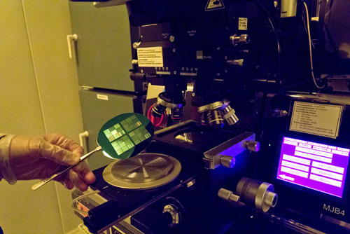
- The demand for thin and ultra-thin crystalline silicon wafers responds to the application possibilities offered by 3D circuit integration of micro-electromechanical systems (MEMS) with conventional microchips and also to the latest generation of ...
today Nanowerk - MEMS technology
- Stealth Dicing Technology for MEMS Applications
- Hence, this technology consists of two processes, namely the 'laser process' which involves the formation of a cleaving start point (SD layer) on the interior of the wafer for splitting it into chips and the 'separation process' which involves the ...
today AZoNano.com - MEMS technology
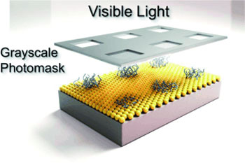
- Polymer Brushes in 3D
- It can also be used in the fabrication of next-generation microelectronic devices. Other areas of application include biocompatible coatings for implants, chemical sensors, and new “intelligent” materials. Although progress has been made with regard to ...
today AZoNano.com - MEMS technology
MEMS business
- Over 0.5B mobile health and fitness sensor shipments in 2017 – report
- “Advances in low power wireless communications, MEMS [micro-electro-mechanical systems] and multi-sensor arrays have resulted in viable body area network applications for clinical patient monitoring, assisted care, at-home chronic disease management ...
yesterday Mobile World Live - MEMS business
- It's a Tie: Bosch and STM Hold Joint Honors as No. 1 MEMS Suppliers for 2012
- (June 10, 2013)-For the first time ever, no clear winner has emerged to claim top honors in the microelectromechanical systems (MEMS) business for 2012, with Bosch of Germany and French-Italian STMicroelectronics ending up evenly splitting the title of No.
today Robotics Tomorrow - MEMS business
- China's GSMC Selects SPTS Rapier Etch System to Manufacture Inertial MEMS ...
- SPTS' results were consistent with their position as the number one supplier to our industry,” said Dr. Qi Li, vice president of purchasing at GSMC. “Their deep understanding of MEMS processing will be valuable as we ramp products through our new line.”.
today AZoNano.com - MEMS business
- MEMS startup wins strategic investment - EE Times
- Qualtre uses bulk-acoustic wave (BAW) disks instead of the usual tuning-fork resonator used in most MEMS gyroscopes, technology that it licensed from the Georgia Institute of Technology. The company was also able to ...
yesterday - MEMS business
Nanotechnology
- Antenna-in-Box Platform for Nanoscale Biochemical Assays with Single ...
- ... zeptoliters (1 zL = 10-21L), realizing a gain of four orders of magnitude as compared to classical microscopes. The antenna-in-box offers a highly efficient platform for nanoscale biochemical assays with single molecule sensitivity at physiological ...
yesterday AZoNano.com - Nanotechnology
 Nanotechnology helps track and improve drug action in pancreatic cancer Nanotechnology helps track and improve drug action in pancreatic cancer
- "Until now, we have been limited to studying tumour signalling in two dimensions – and lacked a dynamic way of reporting on drug targeting in live tumour tissue. Nanotechnology opens up a portal into living tissue that allows us to watch cancers ...
yesterday Science Codex - Nanotechnology
 Will contact lens computers make Google Glass passe? Will contact lens computers make Google Glass passe?
- Researchers were able to create these computers using liquid solutions of the nanomaterials which are put on a spinning surface, like the contact lens, at low temperatures. While the contact lens cannot yet be called a display, the material being used ...
today Tech2 - Nanotechnology
 Brush nanostructures in 3D Brush nanostructures in 3D
- It can also be used in the fabrication of next-generation microelectronic devices. Other areas of application include biocompatible coatings for implants, chemical sensors, and new “intelligent” materials. Although progress has been made with regard to ...
today Nanowerk - Nanotechnology
Featured Event
Call for Papers. Participate at the premier conference for the lithography community. Contribute your latest work in the areas of advanced etch technology for nanopatterning, EUV lithography, microlithography, resist materials, process technologies, and more. For the past 38 years, SPIE Advanced Lithography Symposium has played a key role in bringing the lithography community together to solve challenges required by the semiconductor industry. Abstracts are due September 2013.
Event Calendar
|
|