|
View Mailing Online
MEMS technology
 SCHOTT offers wide product portfolio of glass wafers for semiconductor industry SCHOTT offers wide product portfolio of glass wafers for semiconductor industry
- MEMpax® is a very thin, high-quality borosilicate glass for use in MEMS (micro-electro mechanical systems) technology. It is available in thicknesses from 0.7 mm down to 0.1 mm. Similar to SCHOTT's BOROFLOAT® 33 in terms of physical, thermal and ...
yesterday Glass on Web - MEMS technology
- 10 mindblowingly futuristic technologies that will appear by the 2030s
- These devices, however, are getting steadily smaller owing to the miniaturization revolution that's in full swing (e.g. the shift towards microelectromechanical systems, or MEMS). In short order we'll be living in a Rainbow's End world, where ...
2013-07-05 io9 - MEMS technology
- Unlikely Competitor for Diamond as Best Thermal Conductor : Boron Arsenide ...
- Smaller, faster and more powerful microelectronic devices pose the daunting challenge of removing the heat they generate. Good thermal conductors placed in contact with such devices channel heat rapidly away from unwanted "hot spots" that decrease the ...
today Science Daily (press release) - MEMS technology
- SSEC adds WaferEtch and WaferStorm platforms to single-wafer wet processing ...
- The flagship of the WaferEtch platform, the TSV REVEALER, is specifically configured to address the requirements of TSV reveal (where the backside of the wafer is thinned to reveal the copper interconnects), which has become a target area in the ...
today Semiconductor Today - MEMS technology
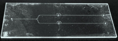
 An all-glass lab-on-a-chip An all-glass lab-on-a-chip
- Yo Tanaka from the RIKEN Quantitative Biology Center has now developed a reliable and durable system for incorporating glass microfluidics into lab-on-a-chip devices ("Electric actuating valves incorporated into an all glass-based microchip exploiting ...
2013-07-04 Nanowerk - MEMS technology
MEMS business
 Bet on a 3-D-printing disruption with this stock Bet on a 3-D-printing disruption with this stock
- The company also offers very specialized laser micro-machining services that command a premium price. XONE has only been trading since its IPO in April, but it has put together a strong chart with no big pullbacks. If the thought of getting in early on ...
2013-07-04 Globe and Mail - MEMS business
- Alchimer Signs Collaboration With CEA-Leti to Evaluate Metallization Processes ...
- Leti is focused on creating value and innovation through technology transfer to its industrial partners. It specializes in nanotechnologies and their applications, from wireless devices and systems, to biology, healthcare and photonics. NEMS and MEMS ...
today Marketwire (press release) - MEMS business
- Advancing MEMS packaging, assembly, and test for the marketplace
- Jun 11, 2013 ... Advancing MEMS packaging, assembly, and test for the marketplace. Because P/ A/T can account for 60% of MEMS cost, finding new ways to ...
www.electronicproducts.com - MEMS business
Nanotechnology
- Nanoelectromechanical sensors (NEMS) based on graphene membranes
- (Nanowerk News) Research results of a research collaboration between the University of Siegen, KTH Royal Institute of Technology (Sweden) and the University of Udine (Italy) have been published in Nano Letters ("Electromechanical Piezoresistive Sensing ...
today Nanowerk - Nanotechnology
 Pollution control with nanotechnology Pollution control with nanotechnology
- Nanotechnologies are particularly suited for treating groundwater aquifers but also contaminated soil at the site of the contamination (in situ). However, in remediation projects (reclamation of contaminated sites), they have only been used hesitantly ...
2013-07-06 Nanowerk - Nanotechnology
 Green graphene band-aid Green graphene band-aid
- Graphene is less of a threat to humans or other mammals because nanosheets become surrounded by serum proteins, says Liu Zengrong of the Institute of Systems Biology in Shanghai, though he acknowledges that nanomaterial toxicity is of 'great concern' ...
today Chemistry World - Nanotechnology
- Nanotechnology researchers find a way for reducing defects in materials
- (Nanowerk News) Researchers from MESA+, the research institute for nanotechnology at the University of Twente, have developed a method to reduce the number of 'defects' in heterogeneous oxide materials. As a result, the electrical conductivity of these ...
2013-07-04 Nanowerk - Nanotechnology
Nanotech business
- Azaya Therapeutics Launches Parexo Labs, Offering Liposomal Manufacture ...
- Azaya Therapeutics Inc., an oncology company focused on developing more effective cancer treatments through its nanotechnology platform, announced the launch of a new division, Parexo Labs, a contract development and manufacturing organization ...
today Wall Street Journal - Nanotech business
- Nano4Life 2013 Conference: Post event report
- Over the past decade we have seen the very significant role that nanotechnologies are playing within the life science industry. With further collaboration between the key players in the supply chain, we can expect to drive forward the convergence of ...
today Nanotechnology News - Nanotech business
Featured Event
The Second Annual InvenSense MotionTracking Developers Conference will again bring together System OEM's, Ecosystem Partners, Application Developers, and Industry Analysts to learn about the technologies, market and future applications for MotionTracking in smartphones, tablets, and health and sports monitoring.
Event Calendar
|
|