|
View Mailing Online
MEMS technology
- NIST shows how to make a compact frequency comb in minutes
- Conventional microfabrication techniques, by contrast, may require hours, days or even weeks. The NIST technique involves laser machining of a quartz rod (a common type of glass) to shape and polish a small, smooth disk within which light can circulate ...
yesterday EurekAlert (press release) - MEMS technology
 Trapped T-Rays Aid Scanners Trapped T-Rays Aid Scanners
- The structure is made of tiny (micro-scale) cavities etched into the surface of silicon. Terahertz waves that hit the structure are captured and compressed inside the cavities. "By tailoring the silicon properties through the use of micro-structures ...
today Laboratory Equipment - MEMS technology
 New Optical Interferometry System for Fast Areal Surface Measurement of ... New Optical Interferometry System for Fast Areal Surface Measurement of ...
- The product is a new optical interferometry system for fast areal surface measurement of microscale and nanoscale surfaces that are immune to environmental noise. The innovative process uses wavelength scanning interferometry together with an ...
today AZoNano.com - MEMS technology
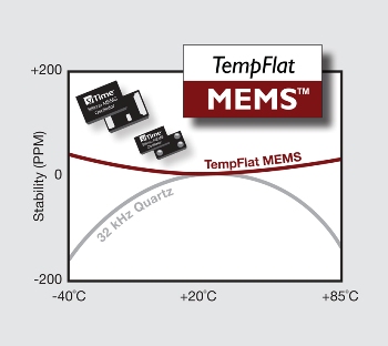
- MEMS Nixes Temperature Compensation
- SiTime is claiming a 30-times boost in stability for its micro-electro-mechanical system (MEMS) oscillators, which it characterizes as "flat" over the entire temperature range. TempFlat oscillators vary as little as 20 parts per million (ppm) today ...
yesterday EE Times - MEMS technology
- Understanding Low-Power IC Design Techniques
- A former MIT graduate student, Patrick Mercier, who is now an assistant professor at the University of San Diego, helped develop an integrated radio transmitter circuit at Microsystems Technology Laboratories of MIT (MTL) powered by this biological ...
yesterday Electronic Design - MEMS technology
 Supercomputers help microfluidics researchers make waves at the microscopic ... Supercomputers help microfluidics researchers make waves at the microscopic ...
- Exploring the phase space of fluid deformations using high throughput computing: Each configuration of microfluidic system (pillar diameter, channel height, and flow speed) results is a specific fluid deformation. XSEDE resources were used to classify ...
today Phys.Org - MEMS technology
 SiTime Introduces TempFlat MEMS That Eliminates Temperature Compensation SiTime Introduces TempFlat MEMS That Eliminates Temperature Compensation
- “SiTime's TempFlat MEMS is an exciting development that enables SiTime to target any precision timing application, without exception. The unbeatable combination of SiTime's TempFlat MEMS technology and semiconductor infrastructure will permanently ...
today AZoNano.com - MEMS technology
MEMS business
- Leti and EV Group launch a Common Lab
- “This project leverages CEA-Leti's global leadership in wafer-bonding research and EVG's unparalleled expertise in developing wafer bonding equipment and process technology.” “Like all common labs that Leti creates with its partners, this project is ...
today electronicsfeed.com - MEMS business
Nanotechnology
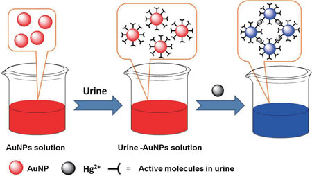
 Bioinspired nanotechnology colorimetric assays - turning trash into treasure Bioinspired nanotechnology colorimetric assays - turning trash into treasure
- (Nanowerk Spotlight) Colorimetric sensing techniques require only the naked eye or ordinary visible color photography and are attractive because of their low cost, use of inexpensive equipment, and above all, their simple-to-understand results ...
today Nanowerk - Nanotechnology
- Nanotechnology researchers image individual atoms in a living catalytic reaction
- (Nanowerk News) Groundbreaking new electron microscopy technology developed at the York JEOL Nanocentre at the University of York is allowing researchers to observe and analyse single atoms, small clusters and nanoparticles in dynamic in-situ ...
today Nanowerk - Nanotechnology
- Novel quantum dot-based technique sees 100 different molecules in a single cell
- The researchers note that because this methodology uses commercially available enzymes and standard fluorescence microscopes, it is relatively low cost. They also plan to automate the procedure using microfluidics and automated image processing ...
today Nanowerk - Nanotechnology
Featured Event
Call for Papers. Participate at the premier conference for the lithography community. Contribute your latest work in the areas of advanced etch technology for nanopatterning, EUV lithography, microlithography, resist materials, process technologies, and more. For the past 38 years, SPIE Advanced Lithography Symposium has played a key role in bringing the lithography community together to solve challenges required by the semiconductor industry. Abstracts are due September 2013.
Event Calendar
|
|