|
View Mailing Online
MEMS technology
- eCompass MEMS combo module comes in a 2x2x1mm package
- STMicroelectronics has unveiled what the company claims to be the world's smallest eCompass combining a 3-axis accelerometer and 3-axis magnetometer in a single package measuring only 2x2x1mm. Designed for advanced navigation and ...
today EDN.com - MEMS technology
- SMI implements Centipede's massively parallel test for MEMS
- Silicon Microstructures, Inc. (SMI) announces test-in-tray for parallel testing of MEMS based pressure sensors in volume production. SMI has put test-in-tray processing into production for automated handling and testing. Pressure, temperature and ...
2013-07-26 electronicsfeed.com - MEMS technology
- Micro-Positioner produces motion with 6 degrees of freedom.
- The hexapod is ideal for many applications including industrial automation and manufacturing, neuroscience, bio-technology research, or for micro-manipulation, the alignment and assembly of mechanical components, micromachining, satellite testing, ...
today ThomasNet News (press release) - MEMS technology
 MEMS – Bringing Digital Music to Life MEMS – Bringing Digital Music to Life
- Another approach would be to use the now ubiquitous microelectromechanical system ( MEMS ). Among myriad other uses, MEMS devices are ubiquitous in cell phones and tablet computers. But they can do a lot more than detect screen orientation. A MEMS ...
2013-07-26 ENGINEERING.com - MEMS technology
- 'Electronic skin' lights up when touched
- ... just 25 µm thick on top of a silicon-wafer substrate and subsequently hardening the plastic by baking it in an oven at 300 °C. The electronic components were then vertically built on top of the plastic surface using conventional microfabrication ...
2013-07-26 physicsworld.com - MEMS technology
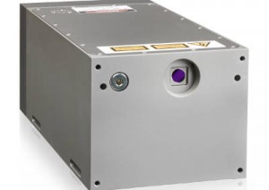
 Micromachining laser delivers 5W Micromachining laser delivers 5W
- 2013/07/26. 07aug13CoherentHelios 400 Coherent is claiming higher micromachining throughput from its Helios series of micromachining lasers when dicing, scribing and marking. With a pulse repetition frequency of 50kHz and a pulse width of under 600ps ...
2013-07-26 ElectronicsWeekly.com - MEMS technology
- Novel material for cooling of electronic devices discovered
- As microelectronic devices become smaller, faster, and more powerful, thermal management is becoming a critical challenge. This work provides new insight into the nature of thermal transport at a quantitative level and predicts a new material, with ...
today Science Daily (press release) - MEMS technology
- The totally implantable cochlear implant history
- They have contracted a company out of the UK (Imperial College Innovations Ltd.) to supply the Micro-electronic speech processors. Dr. Chris Toumazou of the Imperial College of Science, Technology and Medicine developed the speech processing ...
2013-07-26 EE Times - MEMS technology
MEMS business
- Calient Gets $27 Million To Take SDN At Light Speed
- Using 3D MEMS (micro-electromechanical systems) and all optical switches in the data center means that without upgrading the switch, speeds can go from 10Gbps to 40Gbps and then 100 Gbps. To move into a hybrid packet-optical circuit switch network, ...
2013-07-26 Data Center Knowledge - MEMS business
Nanotechnology
 Tetrapod Quantum Dots Light the Way to Stronger Polymers: Berkeley Lab ... Tetrapod Quantum Dots Light the Way to Stronger Polymers: Berkeley Lab ...
- In a study led by Paul Alivisatos, Berkeley Lab director and the Larry and Diane Bock Professor of Nanotechnology at the University of California (UC) Berkeley, the research team incorporated into polymer fibers a population of tetrapod quantum dots ...
today Nanotechnology News (press release) - Nanotechnology
 New Nanoscale Self-Assembling Materials Could Enable Further Chip ... New Nanoscale Self-Assembling Materials Could Enable Further Chip ...
- Nanoscale “giant surfactants” that use nanopatterning to combine functioning molecular nanoparticles with polymer surface films and liquid solutions have been developed by University of Akron. Surfactants are compounds that lower the surface tension ...
today Science World Report - Nanotechnology
- Nanotechnology researchers convert cement into an electrical conductor
- (Nanowerk News) Researchers at the University of Alicante have developed a cementitious material incorporating carbon nanofibers in its composition, turning cement into an excellent conductor of electricity capable of performing functions beyond its ...
today Nanowerk - Nanotechnology
- Nanotechnology advance in making 'programmable matter' using nanocrystals
- The result gives nanotechnology researchers a new tool for controlling how objects one-millionth the size of a grain of sand arrange themselves into useful materials, it gives a means to discover the rules for “programming” them into desired ...
today Nanowerk - Nanotechnology
Featured Event
Call for Papers. Participate at the premier conference for the lithography community. Contribute your latest work in the areas of advanced etch technology for nanopatterning, EUV lithography, microlithography, resist materials, process technologies, and more. For the past 38 years, SPIE Advanced Lithography Symposium has played a key role in bringing the lithography community together to solve challenges required by the semiconductor industry. Abstracts are due September 2013.
Event Calendar
- Enabling Nanofabrication for Rapid Innovation
- 2013-08-18 - 2013-08-21
Napa, CA
|
|
- Shaping the Future of MEMS & Sensors
- 2013-09-10
Santa Clara, CA
|
|
- Trillion Sensors Summit
- 2013-10-23 - 2013-10-25
Stanford, CA
|
|
- AVS 60th International Symposium & Exhibition
- 2013-10-27 - 2013-11-01
Long Beach, CA
|
|
- MicroTAS 2013
- 2013-10-27 - 2013-10-31
Freiburg, Germany
The 17th International Conference on Miniaturized Systems for Chemistry and Life Sciences
|
|
- MIG MEMS Executive Congress U.S.
- 2013-11-07 - 2013-11-08
Napa, CA
Meet your next customer at MEMS Executive Congress!
|
|
- 2013 3D ASIP
- 2013-12-11 - 2013-12-13
Burlingame, CA
3D Architectures for Semiconductor Integration and Packaging
|
|
- The 27th International Conference on Micro Electro Mechanical Systems
- 2014-01-26 - 2014-01-30
San Francisco, CA
|
|
- SPIE Photonics West 2014
- 2014-02-01 - 2014-02-06
San Francisco, CA
|
|
- SPIE Advanced Lithography 2014
- 2014-02-23 - 2014-02-27
San Jose, CA
|
|
|
|