|
View Mailing Online
MEMS technology
 Phone Sensors Could Meld with Human Body Phone Sensors Could Meld with Human Body
- The technology is called microelectromechanical systems, or MEMS, and involves parts less than 100 microns wide, the average diameter of a human hair. For example, the accelerometer that tells a smartphone if its screen is being held vertically or ...
today LiveScience.com - MEMS technology
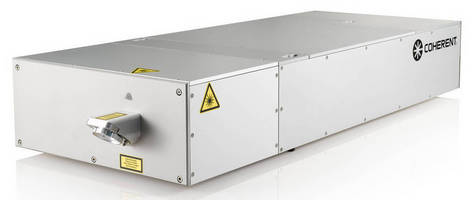
 Industrial Picosecond Lasers enable machining of thick materials. Industrial Picosecond Lasers enable machining of thick materials.
- Talisker lasers are a family of industrial picosecond products, well documented to deliver higher quality process finished goods than conventional pulsed lasers or non-laser micromachining methods. Picosecond lasers achieve the quality improvement ...
yesterday ThomasNet News (press release) - MEMS technology
- On route to building flexible high-performance computers
- The fabrication of p-type metal-oxide–semiconductor field-effect transistors (MOSFETs) by Hussain's team relies solely on standard microfabrication techniques and it is fully compatible with CMOS processing. In a previous Nanowerk Spotlight ...
today Nanowerk - MEMS technology
- Time for a change: Quartz oscillators make way for MEMS
- But this is a market ready for disruption, and quartz is facing challenges from an alternative approach based on MEMS (micro-electromechanical systems) resonator technology. Within the MEMS industry, there are two different technologies competing to ...
yesterday EDN.com - MEMS technology
MEMS business
- Sandia showcases ready-to-license technology
- The lab showcased more than three-dozen products, processes and software in the areas of bioscience, computing and information, energy and climate, and nanodevices and microsystems. The event highlighted some select “hot technologies” with high ...
yesterday Albuquerque Journal (subscription) - MEMS business
- TSMC Licences Soitec's IP Portfolio for BSI Image Sensors
- Today Soitec's IP portfolio contains nearly 3,000 patents covering several technologies for manufacturing engineered wafers and to be used as building blocks in leading-edge microelectronic products such as BSI image sensors. In this case, the back ...
today AZoSensors - MEMS business
- Calient confirms interoperability of OpenFlow API for S320 optical circuit switch
- Based on Calient's proprietary 3D microelectromechanical (MEMS) technology, the S320 optical circuit switch supports up to 320 ports (320 input ports and 320 output ports) and per-port data rates of more than 100 Gbps (see "Calient debuts high-density ...
yesterday LightWave Online (press release) - MEMS business
- Is Apple iPhone 5S Motion Sensor Supplier InvenSense? AAPL INVN ...
- InvenSense's single-chip MotionTracking solutions combine MEMS (micro-electromechanical system) -based motion sensors, such as accelerometers and gyroscopes, with mixed-signal integrated circuits to improve performance, accuracy, and intuitive ...
today Investor's Business Daily - MEMS business
Nanotechnology
- Nanotechnology enabled solar steam generation to disinfect medical ...
- (Nanowerk News) A revolutionary new solar energy technology that turns water into steam without boiling the entire container of water has become the basis for new devices to sanitize medical and dental instruments and human waste in developing ...
yesterday Nanowerk - Nanotechnology
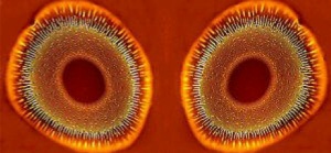
- Local nanoscale electrical measurements for graphene
- Topography of a graphene Hall bar, superimposed with a surface potential map obtained using the FM-KPFM technique. Research from the National Physical Laboratory (NPL), Royal Holloway, University of London, and Linköping University, Sweden, has ...
2013-09-09 Phys.Org - Nanotechnology
 NPL Contributes Nanoscale Images to Guardian's Nanotechnology Blog NPL Contributes Nanoscale Images to Guardian's Nanotechnology Blog
- Scientists from the National Physical Laboratory (NPL) have contributed nanoscale images of bleached hair, gold nanoparticles and the impact of cluster guns to the Guardian's nanotechnology blog, Small World. One of the NPL images shows ...
today AZoNano.com - Nanotechnology
Nanotech business
- LiqTech's Nanotechnology-Based Silicon Carbide Membranes Receive NSF ...
- LiqTech International Inc.,, a clean technology company that manufactures and markets highly specialized filtration technologies, today announced that its silicon carbide (SiC) membranes are now National Sanitation Foundation (NSF) Certified. LiqTech's ...
today AZoNano.com - Nanotech business
Featured Event
Call for Papers. Participate at the premier conference for the lithography community. Contribute your latest work in the areas of advanced etch technology for nanopatterning, EUV lithography, microlithography, resist materials, process technologies, and more. For the past 38 years, SPIE Advanced Lithography Symposium has played a key role in bringing the lithography community together to solve challenges required by the semiconductor industry. Abstracts are due September 2013.
Event Calendar
- MEMS Industry Group Workshop: MEMS and Sensors
- 2013-09-19
University of Berkeley, CA
Enablers for the Internet of Things
|
|
- Automotive Sensors & Electronics Expo 2013
- 2013-10-09
Detroit, Michigan
|
|
- Trillion Sensors Summit
- 2013-10-23 - 2013-10-25
Stanford, CA
|
|
- AVS 60th International Symposium & Exhibition
- 2013-10-27 - 2013-11-01
Long Beach, CA
|
|
- MicroTAS 2013
- 2013-10-27 - 2013-10-31
Freiburg, Germany
The 17th International Conference on Miniaturized Systems for Chemistry and Life Sciences
|
|
- MIG MEMS Executive Congress U.S.
- 2013-11-07 - 2013-11-08
Napa, CA
Meet your next customer at MEMS Executive Congress!
|
|
- 2013 3D ASIP
- 2013-12-11 - 2013-12-13
Burlingame, CA
3D Architectures for Semiconductor Integration and Packaging
|
|
- The 27th International Conference on Micro Electro Mechanical Systems
- 2014-01-26 - 2014-01-30
San Francisco, CA
|
|
- SPIE Photonics West 2014
- 2014-02-01 - 2014-02-06
San Francisco, CA
|
|
- SPIE Advanced Lithography 2014
- 2014-02-23 - 2014-02-27
San Jose, CA
|
|
|
|