|
View Mailing Online
MEMS technology
- Scientists develop human-on-a-chip to research chemical warfare agent exposure
- They are made up of multiple layers of cells growing on a membrane and are connected to each other by microfluidics, tiny micro channels that copy the function of blood vessels. Their primary purpose is to take the place of animal research. “Today, the ...
today R & D Magazine - MEMS technology
 Solar cell developed with highest efficiency ever at 44.7% Solar cell developed with highest efficiency ever at 44.7%
- This four-junction solar cell contains our collected expertise in this area over many years … a new procedure called wafer bonding plays a central role. With this technology, we are able to connect two semiconductor crystals, which otherwise cannot be ...
yesterday SlashGear - MEMS technology
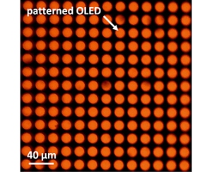
 New Photoresist Technology Enables Submicron Patterns on Organic ... New Photoresist Technology Enables Submicron Patterns on Organic ...
- ... system integration. * Photoresist: Photosensitive materials that cause photochemical reaction due to light exposures, have different developer solubility at exposed parts and unexposed parts, and are used for microfabrication in semiconductor ...
today AZoNano.com - MEMS technology
 Kelvin's water dropper miniaturised on a chip Kelvin's water dropper miniaturised on a chip
- Thomas Jones, a leading researcher in microelectromechanical systems and droplets at the University of Rochester in the US says he believes 'the microfluidic Kelvin dropper may prove to be an icon of microelectromechanical possibilities.' Jones also ...
today Chemistry World - MEMS technology
MEMS business
- PRESS DIGEST-New York Times business news - Sept 26
- A group of Stanford researchers has moved a step closer to answering the question of what happens when silicon, the standard material in today's microelectronic circuits, reaches its fundamental limits for use in increasingly small transistors. In a ...
yesterday Reuters - MEMS business
- Top 12 MEMS Chips Pioneering New Markets
- Micro-electromechanical systems (MEMS) have already revolutionized the consumer market -- from smartphones to tablets -- all of which use multiple MEMS chips to sense orientation, motion, heading, and more. In the coming year, MEMS chips are poised to ...
yesterday EE Times - MEMS business
- LensVector and Hosiden Announce Manufacturing Partnership
- "LensVector's manufacturing strategy is to merge high quality, low cost mature LCD panel manufacturing with our proprietary thin film process. This combination will provide very high capacity from existing Fabs yielding arrays of thousands of lens ...
yesterday Marketwired (press release) - MEMS business
- Status of the MEMS Industry 2013
- In 2012, the IC industry saw a 2% decline, but Yole Développements research reveals the MEMS sector managed another 10% growth to become an $11B business. Analysts expect a 12-13% CAGR through 2018 to create a $22.5B MEMS market, growing to ...
today IT Business Net - MEMS business
Nanotechnology
- Carbon Nano-Computing
- Late last month at Hot Chips, an engineering design conference hosted, coincidentally, at Stanford, the director of the Microsystems Technology Office at DARPA made a stir by discussing the end of silicon electronics. In a keynote, Robert Colwell ...
yesterday MIT Technology Review - Nanotechnology
 Nanotechnology surface modification with graphene enhances water resistance Nanotechnology surface modification with graphene enhances water resistance
- These “nanodrapes” are less than a nanometer thick, chemically inert, and provide a layer of protection without changing the properties of the underlying material. The team of researchers, led by Rensselaer Professor Nikhil Koratkar, demonstrated how ...
today Nanowerk - Nanotechnology
- How to make ceramics that bend without breaking - Nanowerk
- While a micrometer is pretty tiny by most standards, it's actually not so small in the world of nanotechnology. "It's large compared to a lot of what nanotech people work on," Lai says. As such, these materials could be important ...
today - Nanotechnology
 Nanotechnology researchers find new energy storage capabilities between ... Nanotechnology researchers find new energy storage capabilities between ...
- (Nanowerk News) Drexel University nanotechnology researchers are continuing to expand the capabilities and functionalities of a family of two-dimensional materials they discovered that are as thin as a single atom, but have the potential to store ...
today Nanowerk - Nanotechnology
 From trash to treasure: plastic bags to high-tech nanomaterial From trash to treasure: plastic bags to high-tech nanomaterial
- Researchers from the University of Adelaide have developed a process of turning waste non-biodegradable plastic bags into high-tech nanomaterial. The process that the researchers have developed makes use of non-biodegradable plastic grocery bags to ...
today EcoSeed - Nanotechnology
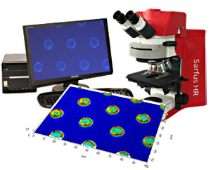
 Sarfus Mapping Nanoscale Microscopy Sarfus Mapping Nanoscale Microscopy
- LE MANS, France, Sept. 26, 2013 — Nanolane is offering its latest generation of Sarfus Mapping stations for label-free, real-time nanoscale life sciences imaging. Sarfus Mapping LR is designed for analyses in air, and Sarfus Mapping HR is suitable for ...
today Photonics.com - Nanotechnology
Featured Event
Currently, each vehicle has an average of 60-100 sensors on board. Because cars are rapidly getting "smarter" the number of sensors is projected to reach as many as 200 sensors per car by 2020. These numbers translate to approximately 22 billion sensors used in the automotive industry per year. This event will bring together leading experts in automotive sensors and electronics who will discuss business and technology issues, ongoing trends, and emerging applications.
Event Calendar
- Automotive Sensors & Electronics Expo 2013
- 2013-10-09
Detroit, Michigan
|
|
- Trillion Sensors Summit
- 2013-10-23 - 2013-10-25
Stanford, CA
|
|
- AVS 60th International Symposium & Exhibition
- 2013-10-27 - 2013-11-01
Long Beach, CA
|
|
- MicroTAS 2013
- 2013-10-27 - 2013-10-31
Freiburg, Germany
The 17th International Conference on Miniaturized Systems for Chemistry and Life Sciences
|
|
- MEMS in Motion Collaboration Summit
- 2013-11-04 - 2013-11-06
Sonoma Renaissance Resort & Spa Hotel, CA, USA
A networking-focused event exclusively for inertial devices
|
|
- MIG MEMS Executive Congress U.S.
- 2013-11-07 - 2013-11-08
Napa, CA
Meet your next customer at MEMS Executive Congress!
|
|
- 2013 3D ASIP
- 2013-12-11 - 2013-12-13
Burlingame, CA
3D Architectures for Semiconductor Integration and Packaging
|
|
- The 27th International Conference on Micro Electro Mechanical Systems
- 2014-01-26 - 2014-01-30
San Francisco, CA
|
|
- SPIE Photonics West 2014
- 2014-02-01 - 2014-02-06
San Francisco, CA
|
|
- SPIE Advanced Lithography 2014
- 2014-02-23 - 2014-02-27
San Jose, CA
|
|
- The 9th Annual IEEE International Conference on Nano/Micro Engineered and Molecular Systems
- 2014-04-13 - 2014-04-16
Honolulu, Hawaii, USA
|
|
|
|